SCES888C May   2018  – May 2024 2N7001T

PRODUCTION DATA  

  1.   1
  2. Features
  3. Applications
  4. Description
  5. Pin Configuration and Functions
  6. Specifications
    1. 5.1 Absolute Maximum Ratings
    2. 5.2 ESD Ratings
    3. 5.3 Recommended Operating Conditions
    4. 5.4 Thermal Information
    5. 5.5 Electrical Characteristics
    6. 5.6 Switching Characteristics
    7. 5.7 Operating Characteristics
    8. 5.8 Typical Characteristics
  7. Parameter Measurement Information
    1. 6.1 Load Circuit and Voltage Waveforms
  8. Detailed Description
    1. 7.1 Overview
    2. 7.2 Functional Block Diagram
    3. 7.3 Feature Description
      1. 7.3.1 Up-Translation or Down-Translation from 1.65 V to 3.60 V
      2. 7.3.2 Balanced CMOS Push-Pull Outputs
      3. 7.3.3 Standard CMOS Inputs
      4. 7.3.4 Negative Clamping Diodes
      5. 7.3.5 Partial Power Down (Ioff)
      6. 7.3.6 Over-voltage Tolerant Inputs
    4. 7.4 Device Functional Modes
  9. Application and Implementation
    1. 8.1 Application Information
    2. 8.2 Typical Applications
      1. 8.2.1 Processor Error Up Translation
        1. 8.2.1.1 Design Requirements
        2. 8.2.1.2 Detailed Design Procedure
        3. 8.2.1.3 Application Curve
      2. 8.2.2 Discrete FET Translation Replacement
    3. 8.3 Power Supply Recommendations
    4. 8.4 Layout
      1. 8.4.1 Layout Guidelines
      2. 8.4.2 Layout Example
  10. Device and Documentation Support
    1. 9.1 Documentation Support
      1. 9.1.1 Related Documentation
    2. 9.2 Receiving Notification of Documentation Updates
    3. 9.3 Support Resources
    4. 9.4 Trademarks
    5. 9.5 Electrostatic Discharge Caution
    6. 9.6 Glossary
  11. 10Revision History
  12. 11Mechanical, Packaging, and Orderable Information

Package Options

Mechanical Data (Package|Pins)
Thermal pad, mechanical data (Package|Pins)
Orderable Information

Load Circuit and Voltage Waveforms

Unless otherwise noted, all input pulses are supplied by generators having the following characteristics:

  • f = 1 MHz
  • ZO = 50 Ω
  • dv/dt ≤ 1 ns/V

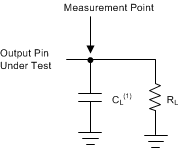
2N7001T Load Circuit
CL includes probe and jig capacitance.
Figure 6-1 Load Circuit
Table 6-1 Load Circuit Conditions
ParameterVCCRLCL
tpdPropagation (delay) time1.65 V – 3.6 V2 kΩ15 pF
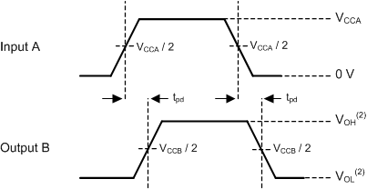
2N7001T Propagation Delay
VCCI is the supply pin associated with the input port.
VOH and VOL are typical output voltage levels that occur with specified RL and CL.
Figure 6-2 Propagation Delay