SNAS483F February 2010 – August 2015 ADC128D818
PRODUCTION DATA.
- 1 Features
- 2 Applications
- 3 Description
- 4 Revision History
- 5 Description (continued)
- 6 Pin Configuration and Functions
- 7 Specifications
-
8 Detailed Description
- 8.1 Overview
- 8.2 Functional Block Diagram
- 8.3 Feature Description
- 8.4 Device Functional Modes
- 8.5 Programming
- 8.6
Register Maps
- 8.6.1 ADC128D818 Internal Registers
- 8.6.2 Configuration Register — Address 00h
- 8.6.3 Interrupt Status Register — Address 01h
- 8.6.4 Interrupt Mask Register — Address 03h
- 8.6.5 Conversion Rate Register — Address 07h
- 8.6.6 Channel Disable Register — Address 08h
- 8.6.7 One-Shot Register — Address 09h
- 8.6.8 Deep Shutdown Register — Address 0Ah
- 8.6.9 Advanced Configuration Register — Address 0Bh
- 8.6.10 Busy Status Register — Address 0Ch
- 8.6.11 Channel Readings Registers — Addresses 20h - 27h
- 8.6.12 Limit Registers — Addresses 2Ah - 39h
- 8.6.13 Manufacturer ID Register — Address 3Eh
- 8.6.14 Revision ID Register — Addresses 3Fh
-
9 Application and Implementation
- 9.1 Application Information
- 9.2
Typical Application
- 9.2.1 Design Requirements
- 9.2.2
Detailed Design Procedure
- 9.2.2.1 Power Management
- 9.2.2.2
Using the ADC128D818
- 9.2.2.2.1 Quick Start
- 9.2.2.2.2 Poweron Reset (POR)
- 9.2.2.2.3 Configuration Register (address 00h)
- 9.2.2.2.4 Interrupt Status Register (address 01h)
- 9.2.2.2.5 Interrupt Mask Register (address 03h)
- 9.2.2.2.6 Conversion Rate Register (address 07h)
- 9.2.2.2.7 One-Shot Register (address 09h)
- 9.2.2.2.8 Deep Shutdown Register (address 0Ah)
- 9.2.2.2.9 Channel Readings Registers (addresses 20h - 27h)
- 9.2.3 Application Curve
- 9.3 System Examples
- 10Power Supply Recommendations
- 11Layout
- 12Device and Documentation Support
- 13Mechanical, Packaging, and Orderable Information
Package Options
Mechanical Data (Package|Pins)
- PW|16
Thermal pad, mechanical data (Package|Pins)
Orderable Information
9 Application and Implementation
NOTE
Information in the following applications sections is not part of the TI component specification, and TI does not warrant its accuracy or completeness. TI’s customers are responsible for determining suitability of components for their purposes. Customers should validate and test their design implementation to confirm system functionality.
9.1 Application Information
9.1.1 Digital Output (DOUT)
The digital output code for a 12-bit ADC can be calculated as:
For Equation 1, ΔVIN = INx – GND, where 0 ≤ x ≤ 7, for the single-ended configuration, and ΔVIN = (IN+ - IN–) for the pseudo-differential configuration. In theory, ΔVIN can be of any value between 0 V and (VREF-3LSb/2). Any ΔVIN value outside of this range will produce a digital output code of 0 or 4095. Figure 32 shows a theoretical plot of DOUT vs. ΔVIN and some sample DOUT calculation using Equation 1.
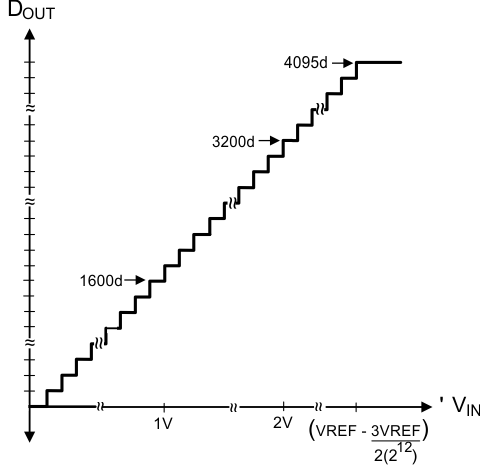 Figure 32. DOUT vs ΔVIN for a 12-Bit ADC Assuming VREF = 2.56 V.
9.1.2 Temperature Measurement System
The ADC128D818 delta-VBE type temperature sensor and delta-sigma ADC perform 9-bit two's-complement conversions of the temperature. This temperature reading can be obtained at the Temperature Reading Register (address 27h). This register is 16-bit wide, and thus, all 9 bits of the temperature reading can be read using a double byte read (Figure 29 or Figure 31). The following Figure 33 and Figure 33 show the theoretical output code (DOUT) vs. temperature and some typical temperature-to-code conversions.
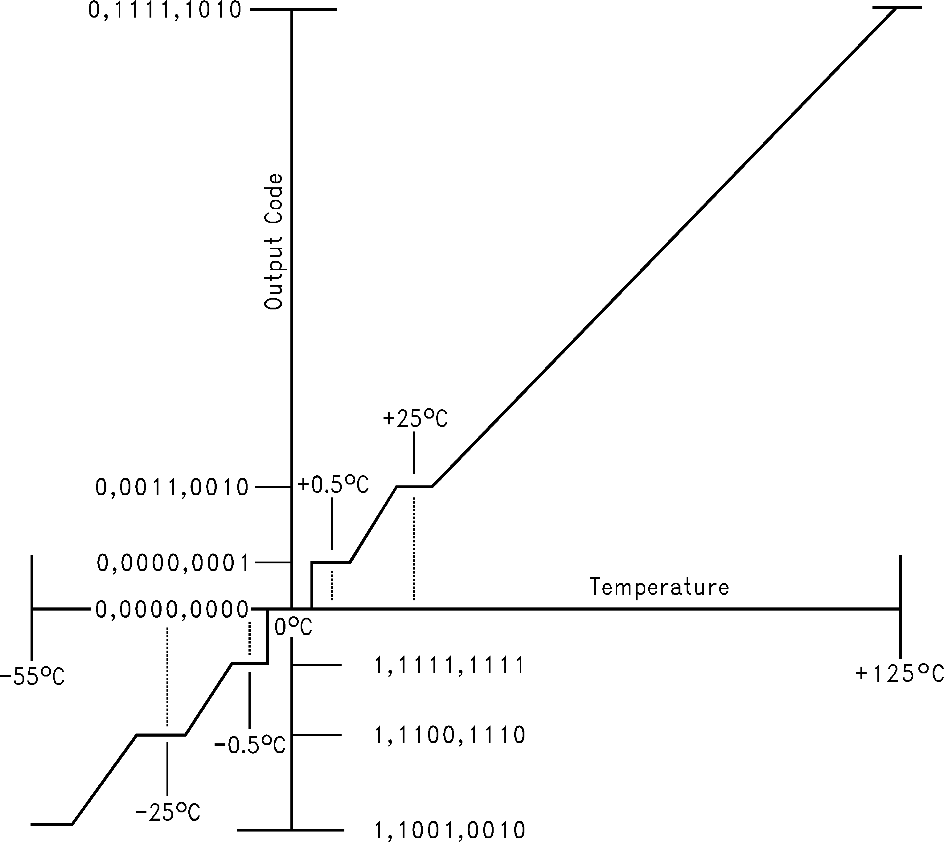
Table 16. Temperature Registers Sample Temperatures
| TEMP | DIGITAL OUTPUT (DOUT) | ||
|---|---|---|---|
| BINARY [MSb...LSb] | DECIMAL | HEX | |
| +125°C | 0 _1111_1010 | 250 | 0_FA |
| +25°C | 0_0011_0010 | 50 | 0_32 |
| +0.5°C | 0_0000_0001 | 1 | 0_01 |
| +0°C | 0_0000_0000 | 0 | 0_00 |
| −0.5°C | 1_1111_1111 | 511 | 1_FF |
| −25°C | 1_1100_1110 | 462 | 1_CE |
| −40°C | 1_1011_0000 | 432 | 1_B0 |
In general, the easiest way to calculate the temperature (°C) is to use the following formulas:
9.1.2.1 Temperature Limits
One of the ADC128D818 features is monitoring the temperature reading. This monitoring is accomplished by setting a temperature limit to the Temperature High Limit Register (Thot , address 38h) and Temperature Hysteresis Limit Register (Thot_hyst, address 39h). When the temperature reading > Thot, an interrupt occurs. How this interrupt occurs will be explained in Temperature Interrupt.
Each temperature limit is represented by an 8-bit, two's complement word with a least significant bit (LSb) equal to 1°C. Table 17 shows some sample temperatures that can be programmed to the Temperature Limit Registers.
In general, use the following equations to calculate the digital code that represents the desired temperature limit:
Table 17. Temperature Limit Registers Sample Temperatures
| TEMP LIMIT | DIGITAL CODE | ||
|---|---|---|---|
| BINARY [MSb...LSb] | DECIMAL | HEX | |
| +125°C | 0111_1101 | 125 | 7D |
| +25°C | 0001_1001 | 25 | 19 |
| +1.0°C | 0000_0001 | 1 | 01 |
| +0°C | 0000_0000 | 0 | 00 |
| −1.0°C | 1111_1111 | 255 | FF |
| −25°C | 1110_1111 | 231 | E7 |
| −40°C | 1101_1000 | 216 | D8 |
9.1.3 Interrupt Structure
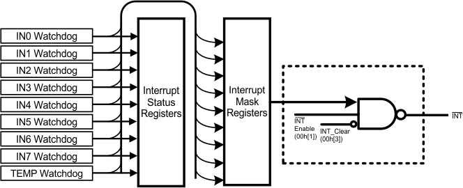 Figure 34. Interrupt Structure
Figure 34 shows the ADC128D818's Interrupt Structure.
NOTE
The number next to each bit name represents its register address and bit number. For example, 'INT_Clear' (00h[3]) refers to bit 3 of register address 00h.
9.1.3.1 Interrupt Output (INT)
ADC128D818 generates an interrupt as a result of each of its internal WATCHDOG registers on the voltage and temperature channels. In general, INT becomes active when all three scenarios, as depicted in Figure 34, occur:
- 'INT_Clear' (00h[3]) = 0.
- 'INT_Enable' (00h[1]) = 1 to enable interrupt output.
- The voltage reading > the voltage high limit or ≤ the voltage low limit, or the temperature reading > Thot.
9.1.3.2 Interrupt Clearing
Reading the Interrupt Status Register (addresses 01h) will output the contents of the register and clear the register. When the Interrupt Status Register clears, the interrupt output pin, INT, also clears until this register is updated by the round-robin monitoring loop.
Another method to clear the interrupt output pin, INT, is setting 'INT_Clear' bit (address 00h, bit 3) = 1. When this bit is high, the ADC128D818 round-robin monitoring loop will stop.
9.1.3.3 Temperature Interrupt
One of the ADC128D818 features is monitoring the temperature reading. This monitoring is accomplished by setting a temperature limit to the Temperature High Limit Register (Thot , address 38h) and Temperature Hysteresis Limit Register (Thot_hyst, address 39h). These limit registers have an interrupt mode, shown in Figure 35, that operates in the following way: if the temperature reading > Thot, an interrupt will occur and will remain active indefinitely until reset by reading the Interrupt Status Register (address 01h) or cleared by the 'INT_Clear' bit.
Once an interrupt event has occurred by crossing Thot, then reset, an interrupt will occur again once the next temperature conversion has completed. The interrupts will continue to occur in this manner until the temperature reading is ≤ Thot_hyst and a read of the Interrupt Status Register has occurred.
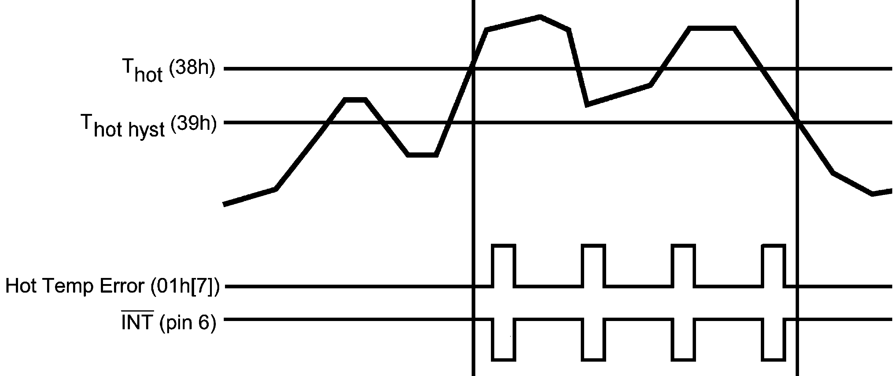 Figure 35. Temperature Response Structure
 (Assuming the Interrupt Output Pin, INT, is Reset Before the Next Temperature Reading)
9.2 Typical Application
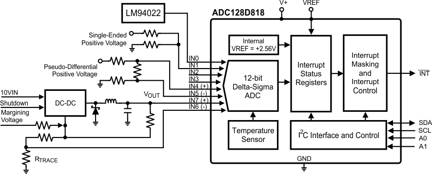 Figure 36. Hardware Monitor Application
9.2.1 Design Requirements
In this typical hardware monitor application, several different sources are being monitored by the ADC128D818. First, an external temperature sensor (LM94022) is being monitored. An external temperature sensor is frequently used to monitor ambient temperature of the system.
9.2.2 Detailed Design Procedure
9.2.2.1 Power Management
To understand the average supply current (I+), the conversion rates must be introduced. ADC128D818 has three types of conversion rates: Continuous Conversion Mode, Low Power Conversion Mode, and One Shot Mode. In the Low Power Conversion Mode, the device converts all of the enabled channels then enters shutdown mode; this process takes approximately 728 ms to complete. (More information on the conversion rate will be discussed in the Conversion Rate Register — Address 07h and One-Shot Register — Address 09h sections).
Each type of conversion produces a different average supply current. The supply current for a voltage conversion will be referred to as I+_VOLTAGE, a temperature conversion as I+_TEMP, and the shutdown mode as I+_SHUTDOWN. These values can be obtained from Typical Performance Characteristics plots.
In general, I+ is the average supply current while ADC128D818 is operating in the Low Power Conversion Mode with all of the available channels enabled. Its plot can be seen in Typical Characteristics and its equation, Equation 6.

where
- a is the number of local temperature available.
- b is the number of ENABLED voltage channel.
Each mode of operation has a different "a" and "b" values. The following table shows the value for "a" and the maximum value for "b" for each mode.
Table 18. "A" and "B" Values
| a | b (MAX) | |
|---|---|---|
| Mode 0 | 1 | 7 |
| Mode 1 | 0 | 8 |
| Mode 2 | 1 | 4 |
| Mode 3 | 1 | 6 |
9.2.2.2 Using the ADC128D818
Table 19. ADC128D818 Internal Registers
| REGISTER NAME | READ/WRITE | REGISTER ADDRESS (HEX) | DEFAULT VALUE [7:0] | REGISTER DESCRIPTION | REGISTER FORMAT |
|---|---|---|---|---|---|
| Configuration Register | R/W | 00h | 0000_1000 | Provides control and configuration | 8-bit |
| Interrupt Status Register | R | 01h | 0000_0000 | Provides status of each WATCHDOG limit or interrupt event | 8-bit |
| Interrupt Mask Register | R/W | 03h | 0000_0000 | Masks the interrupt status from propagating to INT | 8-bit |
| Conversion Rate Register | R/W | 07h | 0000_0000 | Controls the conversion rate | 8-bit |
| Channel Disable Register | R/W | 08h | 0000_0000 | Disables conversion for each voltage or temperature channel | 8-bit |
| One-Shot Register | W | 09h | 0000_0000 | Initiates a single conversion of all enabled channels | 8-bit |
| Deep Shutdown Register | R/W | 0Ah | 0000_0000 | Enables deep shutdown mode | 8-bit |
| Advanced Configuration Register | R/W | 0Bh | 0000_0000 | Selects internal or external VREF and modes of operation | 8-bit |
| Busy Status Register | R | 0Ch | 0000_0010 | Reflects the ADC128D818 'Busy' and 'Not Ready' statuses | 8-bit |
| Channel Readings Registers | R | 20h - 27h | - - - | Report channels (voltage or temperature) readings | 16-bit |
| Limit Registers | R/W | 2Ah - 39h | - - - | Set the limits for the voltage and temperature channels | 8-bit |
| Manufacturer ID Register | R | 3Eh | 0000_0001 | Reports the manufacturer's ID | 8-bit |
| Revision ID Register | R | 3Fh | 0000_1001 | Reports the revision's ID | 8-bit |
9.2.2.2.1 Quick Start
- Power on the device, then wait for at least 33ms.
- Read the Busy Status Register (address 0Ch). If the 'Not Ready' bit = 1, then increase the wait time until 'Not Ready' bit = 0 before proceeding to the next step.
- Program the Advanced Configuration Register — Address 0Bh:
- a. Choose to use the internal or external VREF (bit 0).
- b. Choose the mode of operation (bits [2:1]).
- Program the Conversion Rate Register (address 07h).
- Choose to enable or disable the channels using the Channel Disable Register (address 08h).
- Using the Interrupt Mask Register (address 03h), choose to mask or not to mask the interrupt status from propagating to the interrupt output pin, INT.
- Program the Limit Registers (addresses 2Ah – 39h).
- Set the ‘START’ bit of the Configuration Register (address 00h, bit 0) to 1.
- Set the 'INT_Clear' bit (address 00h, bit 3) to 0. If needed, program the 'INT_Enable' bit (address 00h, bit 1) to 1 to enable the INT output.
The ADC128D818 then performs a round-robin monitoring of enabled voltage and temperature channels. The sequence of items being monitored corresponds to locations in the Channel Readings Registers (except for the temperature reading). Detailed descriptions of the register map can be found at the end of this data sheet.
9.2.2.2.2 Poweron Reset (POR)
When power is first applied, the ADC128D818 performs a power on reset (POR) on several of its registers, which sets the registers to their default values. These default values are shown in Table 19 or in Register Maps.
Registers whose default values are not shown have power on conditions that are indeterminate.
9.2.2.2.3 Configuration Register (address 00h)
The Configuration Register (address 00h) provides all control to the ADC128D818. After POR, the 'START' bit (bit 0) is set low and the 'INT_Clear' bit (bit 3) is set high.
The Configuration Register has the ability to start and stop the ADC128D818, enable and disable the INT output, and set the registers to their default values.
- Bit 0, ‘START’, controls the monitoring loop of the ADC128D818. After POR, set this bit high to start conversion. Setting this bit low stops the ADC128D818 monitoring loop and puts the ADC128D818 in shutdown mode; thus, reducing power consumption. Even though this bit is set low, serial bus communication is possible with any register in the ADC128D818.
- After an interrupt occurs, the INT pin will not be cleared if the user sets this bit low.
- Bit 1, 'INT_Enable', enables the interrupt output pin, INT, when this bit is set high.
- Bit 3, 'INT_Clear', clears the interrupt output pin, INT, when this bit is set high. When this bit is set high, the ADC128D818 monitoring function will stop. The content of the Interrupt Status Register (address 01h) will not be affected.
- Bit 7, ‘INITIALIZATION’, accomplishes the same function as POR, that is, it initializes some of the registers to their default values. This bit automatically clears after being set high. Setting this bit high, however, does not reset the Channel Readings Registers (addresses 20h - 27h) and the Limit Registers (addresses 2Ah - 39h). These registers will be indeterminate immediately after power on. If the Channel Readings Registers contain valid conversion results and/or the Limit Registers have been previously set, they will not be affected by this bit.
9.2.2.2.4 Interrupt Status Register (address 01h)
Each bit in this read-only register indicates whether the voltage reading > the voltage high limit or ≤ the voltage low limit, or the temperature reading > the temperature high limit. For example, if "IN0 High Limit" register (address 2Ah) were set to 2 V and if IN0 reading (address 20h) were 2.56 V, then bit 'IN0 Error' would be 1, indicating that the voltage high limit has been exceeded.
9.2.2.2.5 Interrupt Mask Register (address 03h)
This register masks the interrupt status from propagating to the interrupt output pin, INT. For example, if bit 'IN0 Mask' = 1, then the interrupt output pin, INT, would not be pulled low even if an error event occurs at IN0.
9.2.2.2.6 Conversion Rate Register (address 07h)
There are three options for controlling the conversion rate. The first option is called the Low Power Conversion Mode, where the device converts all of the enabled channels then enters shutdown mode. This process takes approximately 728 ms to complete.
The second option is the Continuous Conversion Mode, where the device continuously converts the enabled channels, thus never entering shutdown mode. A voltage conversion takes 12.2 ms, and a temperature conversion takes 3.6 ms. For example, if operating in mode 2 and three voltage channels were enabled, then each round-robin monitor would take 40.2 ms (3 x 12.2ms + 3.6ms) to complete. Use the "Channel Disable Register" (address 08h) to disable the desired channel(s).
The third option is called the ON-Shot mode, which will be discussed in the next subsection.
9.2.2.2.7 One-Shot Register (address 09h)
The One-Shot register is used to initiate a single conversion and comparison cycle when the device is in shutdown mode or deep shutdown mode, after which the device returns to the respective mode it was in. The obvious advantage of using this mode is lower power consumption because the device is operating in shutdown or deep shutdown mode.
This register is not a data register, and it is the write operation that causes the one-shot conversion. The data written to this address is irrelevant and is not stored. A zero will always be read from this register.
9.2.2.2.8 Deep Shutdown Register (address 0Ah)
The ADC128D818 can be placed in deep shutdown mode, thus reducing more power consumption. The procedures for deep shutdown entrance are:
- Enter shutdown by setting the ‘START’ bit of the “Configuration Register’ (address 00h, bit 0) to 0.
- Enter deep shutdown by setting the ‘DEEP SHUTDOWN’ bit (address 0Ah, bit 0) to 1.
- A one-shot conversion can be triggered by writing any values to register address 09h.
Deep Shutdown Exit Procedure:
- Set the ‘DEEP SHUTDOWN’ bit to 0.
9.2.2.2.9 Channel Readings Registers (addresses 20h - 27h)
The channel conversion readings are available in registers 20h to 27h. Each register is 16-bit wide to accommodate the 12-bit voltage reading or 9-bit temperature reading. Conversions can be read at any time and will provide the result of the last conversion. If a conversion is in progress while a communication is started, that conversion will be completed, and the Channel Reading Registers will not be updated until the communication is complete.
9.2.3 Application Curve
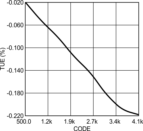 Figure 37. Total Unadjusted Error
9.3 System Examples
9.3.1 General Voltage Monitoring
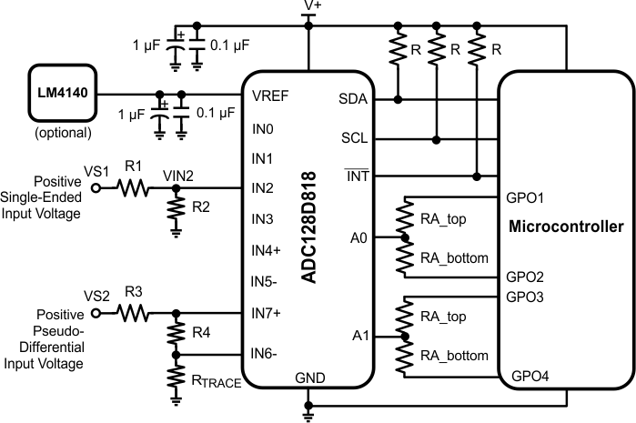 Figure 38. Typical Analog Input Application
A typical application for ADC128D818 is voltage monitoring. In this application, the inputs would most often be connected to linear power supplies of 2.5-V, 3.3-V, ±5-V and ±12-V inputs. These inputs must be attenuated with external resistors to any desired value within the input range. The attenuation is done with resistors R1 and R2 for the positive single-ended voltage, and R3 and R4 for the positive pseudo-differential voltage.
A typical single-ended application might select the input voltage divider to provide 1.9 V at the analog input of the ADC128D818. This is sufficiently high for good resolution of the voltage, yet leaves headroom for upward excursions from the supply of about 25%. To simplify the process of resistor selection, set the value of R2 first. Select a value for R2 between 10 kΩ and 100 kΩ. This is low enough to avoid errors due to input leakage currents yet high enough to protect both the inputs under and overdrive conditions as well as minimize loading of the source. Finally, calculate R1 to provide a 1.9-V input using simple voltage divider derived formula:
Take care to bypass V+ with decoupling 0.1-µF ceramic capacitor and 1-µF tantalum capacitor. If using the external reference option, VREF must be connected to a voltage reference, such as the LM4140, and must also be decoupled to the ground plane by a 0.1-µF ceramic capacitor and a 1-µF tantalum capacitor. For both supplies, the 0.1-µF capacitor must be located as close as possible to the ADC128D818.
Since SDA, SCL, and INT are open-drain pins, they must have external pullup resistors to ensure that the bus is pulled high until a master device or slave device sinks enough current to pull the bus low. A typical pullup resistor, R, ranges from 1.1 kΩ to 10 kΩ. Refer to NXP's "I2C-Bus Specification and User Manual" for more information on sizing R.
Because there are two tri-level address pins (A0 and A1), up to 9 devices can share the same I2C bus. A trick to set these serial addresses uses four GPO (general purpose output) pins from the master device as shown in the example diagram. Table 20 shows how to program these GPO pins.
Table 20. Setting Serial Bus Address Using GPO
| A1 | A0 | GPO1 | GPO2 | GPO3 | GPO4 |
|---|---|---|---|---|---|
| LOW | LOW | Z | LOW | Z | LOW |
| LOW | MID | Z | LOW | HIGH | LOW |
| LOW | HIGH | Z | LOW | HIGH | Z |
| MID | LOW | HIGH | LOW | Z | LOW |
| MID | MID | HIGH | LOW | HIGH | LOW |
| MID | HIGH | HIGH | LOW | HIGH | Z |
| HIGH | LOW | HIGH | Z | Z | LOW |
| HIGH | MID | HIGH | Z | HIGH | LOW |
| HIGH | HIGH | HIGH | Z | HIGH | Z |
9.3.2 Voltage Monitoring for Power Supplies
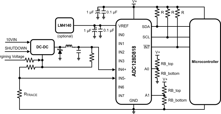 Figure 39. Power Supply Application
Figure 39 shows a more complete systems application using a DC–DC converter. Such configuration can be used in a power supply application. The point to make with this example diagram is the Serial Bus Address connections. The previous example shows A0 and A1 connected to four GPOs, but this example shows a simpler A0 and A1 connection using two resistor dividers. This connection accomplishes the same goal as the GPO connection, that is, it can set A0 and A1 high, low, or to midscale.
For example, to set A0 high, don't populate RB_bottom; to set A0 low, don't populate RB_top; and to set A0 to midscale, leave RB_top and RB_bottom as is and set them equal to each other. A typical RB value ranges from 1 kOhm to 10 kOhm.
9.3.3 Temperature Sensors
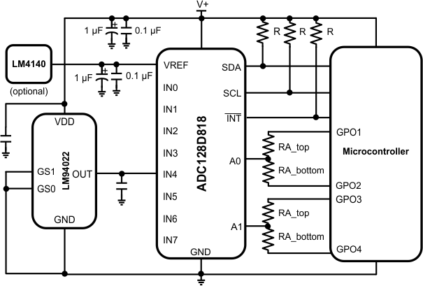 Figure 40. Temperature Sensor Applications
An external temperature sensor can be connected to any of ADC128D818's eight single-ended input for additional temperature sensing. One such temperature sensor can be TI's LM94022, a precision analog temperature sensor with selectable gains. The application diagram shows LM94022's gains (GS1 and GS0) both grounded indicating the lowest gain setting. Four possible gains can be set using these GS1 and GS0 pins.
According to the LM94022 data sheet (SNIS140), the voltage-to-temperature output plot can be determined using the method of linear approximation as follows:
where
- V is in mV
- T is in °C
- V1 and T1 are the coordinates of the lowest temperature
- and T2 and V2 are the coordinates of the highest temperature.
For example, to determine the equation of a line over a temperature range of 20°C to 50°C, first find V1 and V2 relative to those temperatures, then use Equation 8 to find the transfer function.
For more information and explanation of this example, refer to the LM94022 (SNIS140) data sheet.
9.3.4 Bridge Sensors
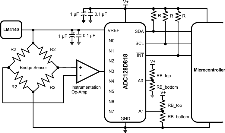 Figure 41. Bridge Sensor Application
ADC128D818 is perfect for transducer applications such as pressure sensors. These sensors measure pressure of gases or liquids and produce a pressure-equivalent voltage at their outputs. Figure 41 shows a typical connection of a pressure sensor, represented by the bridge sensor.
Most pressure sensor has a low sensitivity characteristic, which means its output is typically in the millivolts range. Because of that reason, an op-amp, such as an instrumentation amplifier, can be used for the gain stage.
The positive aspect of this configuration is its ratiometric connection. A ratiometric connection is when the ADC’s VREF and GND are connected to the bridge sensor’s voltage references. With a ratiometric configuration, external VREF accuracy can be ignored.