SBAS526D November   2012  – September 2019 ADS1018

PRODUCTION DATA.  

  1. Features
  2. Applications
  3. Description
    1.     Device Images
      1.      K-Type Thermocouple Measurement Using Integrated Temperature Sensor for Cold-Junction Compensation
  4. Revision History
  5. Device Comparison Table
  6. Pin Configuration and Functions
    1.     Pin Functions
  7. Specifications
    1. 7.1 Absolute Maximum Ratings
    2. 7.2 ESD Ratings
    3. 7.3 Recommended Operating Conditions
    4. 7.4 Thermal Information
    5. 7.5 Electrical Characteristics
    6. 7.6 Timing Requirements: Serial Interface
    7. 7.7 Switching Characteristics: Serial Interface
    8. 7.8 Typical Characteristics
  8. Detailed Description
    1. 8.1 Overview
    2. 8.2 Functional Block Diagram
    3. 8.3 Feature Description
      1. 8.3.1 Multiplexer
      2. 8.3.2 Analog Inputs
      3. 8.3.3 Full-Scale Range (FSR) and LSB Size
      4. 8.3.4 Voltage Reference
      5. 8.3.5 Oscillator
      6. 8.3.6 Temperature Sensor
        1. 8.3.6.1 Converting from Temperature to Digital Codes
        2. 8.3.6.2 Converting from Digital Codes to Temperature
    4. 8.4 Device Functional Modes
      1. 8.4.1 Reset and Power-Up
      2. 8.4.2 Operating Modes
        1. 8.4.2.1 Single-Shot Mode and Power-Down
        2. 8.4.2.2 Continuous-Conversion Mode
      3. 8.4.3 Duty Cycling for Low Power
    5. 8.5 Programming
      1. 8.5.1 Serial Interface
      2. 8.5.2 Chip Select (CS)
      3. 8.5.3 Serial Clock (SCLK)
      4. 8.5.4 Data Input (DIN)
      5. 8.5.5 Data Output and Data Ready (DOUT/DRDY)
      6. 8.5.6 Data Format
      7. 8.5.7 Data Retrieval
        1. 8.5.7.1 32-Bit Data Transmission Cycle
        2. 8.5.7.2 16-Bit Data Transmission Cycle
    6. 8.6 Register Maps
      1. 8.6.1 Conversion Register [reset = 0000h]
        1. Table 4. Conversion Register Field Descriptions
      2. 8.6.2 Config Register [reset = 058Bh]
        1. Table 5. Config Register Field Descriptions
  9. Application and Implementation
    1. 9.1 Application Information
      1. 9.1.1 Serial Interface Connections
      2. 9.1.2 GPIO Ports for Communication
      3. 9.1.3 Analog Input Filtering
      4. 9.1.4 Single-Ended Inputs
      5. 9.1.5 Connecting Multiple Devices
      6. 9.1.6 Pseudo Code Example
    2. 9.2 Typical Application
      1. 9.2.1 Design Requirements
      2. 9.2.2 Detailed Design Procedure
      3. 9.2.3 Application Curves
  10. 10Power Supply Recommendations
    1. 10.1 Power-Supply Sequencing
    2. 10.2 Power-Supply Decoupling
  11. 11Layout
    1. 11.1 Layout Guidelines
    2. 11.2 Layout Example
  12. 12Device and Documentation Support
    1. 12.1 Documentation Support
      1. 12.1.1 Related Documentation
    2. 12.2 Receiving Notification of Documentation Updates
    3. 12.3 Community Resources
    4. 12.4 Trademarks
    5. 12.5 Electrostatic Discharge Caution
    6. 12.6 Glossary
  13. 13Mechanical, Packaging, and Orderable Information

Package Options

Mechanical Data (Package|Pins)
Thermal pad, mechanical data (Package|Pins)
Orderable Information

Power-Supply Decoupling

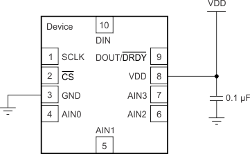
Good power-supply decoupling is important to achieve optimum performance. VDD must be decoupled with at least a 0.1-µF capacitor, as shown in Figure 27. The 0.1-μF bypass capacitor supplies the momentary bursts of extra current required from the supply when the ADS1018 is converting. Place the bypass capacitor as close to the power-supply pin of the device as possible using low-impedance connections. For best performance, use multilayer ceramic chip capacitors (MLCCs) that offer low equivalent series resistance (ESR) and inductance (ESL) characteristics for power-supply decoupling purposes. For very sensitive systems, or for systems in harsh noise environments, avoiding the use of vias for connecting the capacitors to the device pins may offer superior noise immunity. The use of multiple vias in parallel lowers the overall inductance and is beneficial for connections to ground planes.
ADS1018 ai_1end_inputs_bas457.gifFigure 27. Power-Supply Decoupling