SLAS669E September   2010  – may 2020 ADS5400-SP

PRODUCTION DATA.  

  1. Features
  2. Applications
  3. Description
    1.     Block Diagram
  4. Revision History
  5. Pin Configuration and Functions
    1.     Pin Functions
  6. Specifications
    1. 6.1 Absolute Maximum Ratings
    2. 6.2 ESD Ratings
    3. 6.3 Recommended Operating Conditions
    4. 6.4 Thermal Information
    5. 6.5 Electrical Characteristics
    6. 6.6 Switching Characteristics
    7. 6.7 Timing Characteristics
    8. 6.8 Interleaving Adjustments
    9. 6.9 Typical Characteristics
  7. Detailed Description
    1. 7.1 Overview
    2. 7.2 Functional Block Diagram
    3. 7.3 Feature Description
      1. 7.3.1  Input Configuration
      2. 7.3.2  Voltage Reference
      3. 7.3.3  Analog Input Over-Range Recovery Error
      4. 7.3.4  Clock Inputs
      5. 7.3.5  Over Range
      6. 7.3.6  Data Scramble
      7. 7.3.7  Test Patterns
      8. 7.3.8  Die Identification and Revision
      9. 7.3.9  Die Temperature Sensor
      10. 7.3.10 Interleaving
        1. 7.3.10.1 Gain Adjustment
        2. 7.3.10.2 Offset Adjustment
        3. 7.3.10.3 Input Clock Coarse Phase Adjustment
        4. 7.3.10.4 Input Clock Fine Phase Adjustment
    4. 7.4 Device Functional Modes
      1. 7.4.1 Output Bus and Clock Options
      2. 7.4.2 Reset and Synchronization
      3. 7.4.3 LVDS
    5. 7.5 Programming
      1. 7.5.1 Serial Interface
        1. Table 2. Instruction Byte of the Serial Interface
    6. 7.6 Serial Register Map
      1. 7.6.1 Description of Serial Registers
  8. Application and Implementation
    1. 8.1 Application Information
    2. 8.2 Typical Application
      1. 8.2.1 Design Requirements
      2. 8.2.2 Detailed Design Procedure
        1. 8.2.2.1 Clocking Source for ADS5400-SP
        2. 8.2.2.2 Amplifier Selection
      3. 8.2.3 Application Curve
  9. Power Supply Recommendations
  10. 10Layout
    1. 10.1 Layout Guidelines
    2. 10.2 Layout Example
  11. 11Device and Documentation Support
    1. 11.1 Device Support
      1. 11.1.1 Device Nomenclature
        1. 11.1.1.1 Definition of Specifications
    2. 11.2 Documentation Support
    3. 11.3 Receiving Notification of Documentation Updates
    4. 11.4 Support Resources
    5. 11.5 Trademarks
    6. 11.6 Electrostatic Discharge Caution
    7. 11.7 Glossary
  12. 12Mechanical, Packaging, and Orderable Information

Package Options

Mechanical Data (Package|Pins)
Thermal pad, mechanical data (Package|Pins)
Orderable Information

Application Curve

Figure 40 shows the SNR of the ADC as a function of clock jitter and input frequency for the device. This plot of curves take into account the aperture jitter of the ADC, the number of bits of resolution, and the thermal noise estimation so that Figure 40 may be used to predict SNR for a given input frequency and external clock jitter. Figure 40 then may be used to set the jitter requirement for the clocking solution for a given input bandwidth and given design goal for SNR.
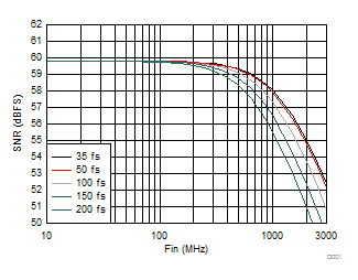
ADS5400-SP D001_SLAS611.gifFigure 40. SNR vs Input Frequency and External Clock Jitter