SLAS946B April 2013 – January 2016 ADS5401
PRODUCTION DATA.
- 1 Features
- 2 Applications
- 3 Description
- 4 Revision History
- 5 Device Options
- 6 Pin Configuration and Functions
-
7 Specifications
- 7.1 Absolute Maximum Ratings
- 7.2 ESD Ratings
- 7.3 Recommended Operating Conditions
- 7.4 Thermal Information
- 7.5 Electrical Characteristics - Supply, Power Supply
- 7.6 Electrical Characteristics - Analog Inputs, Dynamic Accuracy, Clock Input
- 7.7 Electrical Characteristics - Dynamic AC, Enabled
- 7.8 Electrical Characteristics- Dynamic AC, Disabled
- 7.9 Electrical Characteristics - Over-Drive Recovery Error, Sample Timing
- 7.10 Electrical Characteristics - Digital Inputs, Digital Outputs
- 7.11 Serial Register Write Timing Requirements
- 7.12 Reset Timing Requirements
- 7.13 Typical Characteristics
-
8 Detailed Description
- 8.1 Overview
- 8.2 Functional Block Diagram
- 8.3 Feature Description
- 8.4 Device Functional Modes
- 8.5 Programming
- 8.6
Register Maps
- 8.6.1 Register Name: Config0 - Address: 0×00, Default = 0×00
- 8.6.2 Register Name: Config1 - Address: 0×01, Default = 0×00
- 8.6.3 Register Name: Config2 - Address: 0×02, Default = 0×780
- 8.6.4 Register Name: 3 - Address: 0x03
- 8.6.5 Register Name: E - Address: 0x0E
- 8.6.6 Register Name: F - Address: 0x0F
- 8.6.7 Register Name: 2B - Address: 0x2B
- 8.6.8 Register Name: 2C - Address: 0x2C
- 8.6.9 Register Name: 37 - Address: 0x37
- 8.6.10 Register Name: 38 - Address: 0x38
- 8.6.11 Register Name: 3A - Address: 0x3A
- 8.6.12 Register Name: 66 - Address: 0x66
- 9 Application and Implementation
- 10Power Supply Recommendations
- 11Layout
- 12Device and Documentation Support
- 13Mechanical, Packaging, and Orderable Information
Package Options
Mechanical Data (Package|Pins)
- ZAY|196
Thermal pad, mechanical data (Package|Pins)
Orderable Information
1 Features
2 Applications
- Test and Measurement Instrumentation
- Ultra-Wide Band Software Defined Radio
- Data Acquisition
- Power Amplifier Linearization
- Signal Intelligence and Jamming
- Radar and Satellite Systems
- Microwave Receivers
- Cable Infrastructure
- Non-Destructive Testing
- Power Dissipation: 1.33 W/ch
- Spectral Performance at fin = 230 MHz IF
- SNR: 61.3 dBFS
- SFDR: 74 dBc
- Spectral Performance at fin = 700 MHz IF
- SNR: 59.8 dBFS
- SFDR: 69 dBc
3 Description
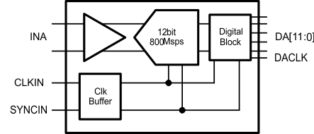
The ADS5401 device is a high-linearity single-channel 12-bit, 800-Msps analog-to-digital converter (ADC) easing front-end filter design for wide bandwidth receivers. The analog input buffer isolates the internal switching of the on-chip track-and-hold from disturbing the signal source as well as providing a high-impedance input. Optionally the output data can be decimated by two. Designed for high SFDR, the ADC has low-noise performance and outstanding spurious-free dynamic range over a large input-frequency range. The device is available in a 196-pin BGA package and is specified over the full industrial temperature range (–40°C to 85°C).
Device Information(1)
| PART NUMBER | PACKAGE | BODY SIZE (NOM) |
|---|---|---|
| ADS5401 | NFBGA (196) | 12.00 mm x 12.00 mm |
- For all available packages, see the orderable addendum at the end of the data sheet.
Simplified Schematic
