SLAS946B April 2013 – January 2016 ADS5401
PRODUCTION DATA.
- 1 Features
- 2 Applications
- 3 Description
- 4 Revision History
- 5 Device Options
- 6 Pin Configuration and Functions
-
7 Specifications
- 7.1 Absolute Maximum Ratings
- 7.2 ESD Ratings
- 7.3 Recommended Operating Conditions
- 7.4 Thermal Information
- 7.5 Electrical Characteristics - Supply, Power Supply
- 7.6 Electrical Characteristics - Analog Inputs, Dynamic Accuracy, Clock Input
- 7.7 Electrical Characteristics - Dynamic AC, Enabled
- 7.8 Electrical Characteristics- Dynamic AC, Disabled
- 7.9 Electrical Characteristics - Over-Drive Recovery Error, Sample Timing
- 7.10 Electrical Characteristics - Digital Inputs, Digital Outputs
- 7.11 Serial Register Write Timing Requirements
- 7.12 Reset Timing Requirements
- 7.13 Typical Characteristics
-
8 Detailed Description
- 8.1 Overview
- 8.2 Functional Block Diagram
- 8.3 Feature Description
- 8.4 Device Functional Modes
- 8.5 Programming
- 8.6
Register Maps
- 8.6.1 Register Name: Config0 - Address: 0×00, Default = 0×00
- 8.6.2 Register Name: Config1 - Address: 0×01, Default = 0×00
- 8.6.3 Register Name: Config2 - Address: 0×02, Default = 0×780
- 8.6.4 Register Name: 3 - Address: 0x03
- 8.6.5 Register Name: E - Address: 0x0E
- 8.6.6 Register Name: F - Address: 0x0F
- 8.6.7 Register Name: 2B - Address: 0x2B
- 8.6.8 Register Name: 2C - Address: 0x2C
- 8.6.9 Register Name: 37 - Address: 0x37
- 8.6.10 Register Name: 38 - Address: 0x38
- 8.6.11 Register Name: 3A - Address: 0x3A
- 8.6.12 Register Name: 66 - Address: 0x66
- 9 Application and Implementation
- 10Power Supply Recommendations
- 11Layout
- 12Device and Documentation Support
- 13Mechanical, Packaging, and Orderable Information
Package Options
Mechanical Data (Package|Pins)
- ZAY|196
Thermal pad, mechanical data (Package|Pins)
Orderable Information
8 Detailed Description
8.1 Overview
The ADS5401 is a wide bandwidth 12-bit 800-Msps single-channel ADC. Designed for high SFDR, the ADS has low-noise performance and outstanding spurious-free dynamic range over a large input frequency. The buffered analog input provides uniform input impedance across a wide frequency range while minimizing sample-and-hold glitch energy. The ADC also provides an option to decimate the output data by two.
8.2 Functional Block Diagram
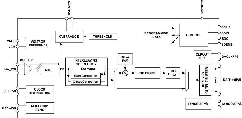
8.3 Feature Description
8.3.1 Test Pattern Output
The ADS5401 can be configured to output different test patterns that can be used to verify the digital interface is connected and working properly. To enable test pattern mode, high performance mode 1 has to be disabled first through a SPI register write. Then different test patterns can be selected by configuring registers x3C, x3D and x3E. All three registers must be configured for the test pattern to work properly.
First set HP1 = 0 (Addr 0x01, D01).
Table 1. Test Pattern Register Configurations
| REGISTER ADDRESS | ALL 0s | ALL 1s | TOGGLE (0xAAA => 0x555) | TOGGLE (0xFFF => 0x000) |
|---|---|---|---|---|
| 0x3C | 0x8000 | 0xBFFC | 0x9554 | 0xBFFC |
| 0x3D | 0x0000 | 0x3FFC | 0x2AA8 | 0x0000 |
| 0x3E | 0x0000 | 0x3FFC | 0x1554 | 0x3FFC |
Table 2. Custom Test Patterns
| REGISTER ADDRESS | CUSTOM PATTERN | |||||||||||||||
|---|---|---|---|---|---|---|---|---|---|---|---|---|---|---|---|---|
| D15 | D14 | D13 | D12 | D11 | D10 | D9 | D8 | D7 | D6 | D5 | D4 | D3 | D2 | D1 | D0 | |
| x3C | 1 | 0 | D11 | D10 | D9 | D8 | D7 | D6 | D5 | D4 | D3 | D2 | D1 | D0 | 0 | 0 |
| x3D | 0 | 0 | 0 | 0 | ||||||||||||
| x3E | 0 | 0 | 0 | 0 | ||||||||||||
For normal operation, set HP1 = 1 (Addr 0x01, D01) and 0x3C, 0x3D, 0x3E all to 0.
8.3.2 Clock Input
The ADS5401 clock input can be driven differentially with a sine wave, LVPECL or LVDS source with little or no difference in performance. The common-mode voltage of the clock input is set to 0.9 V using internal 2-kΩ resistors. This allows for AC coupling of the clock inputs. The termination resistors should be placed as close as possible to the clock inputs in order to minimize signal reflections and jitter degradation.
 Figure 36. Recommended Differential Clock Driving Circuit
8.3.3 Analog Inputs
The ADS5401 analog signal input is designed to be driven differentially. The analog input pins have internal analog buffers that drive the sampling circuit. As a result of the analog buffer, the input pins present a high impedance input across a very wide frequency range to the external driving source which enables great flexibility in the external analog filter design as well as excellent 50-Ω matching for RF applications. The buffer also helps to isolate the external driving circuit from the internal switching currents of the sampling circuit which results in a more constant SFDR performance across input frequencies.
The common-mode voltage of the signal input is internally biased to 1.9 V using 500-Ω resistors which allows for AC coupling of the input drive network. Each input pin (INP, INM) must swing symmetrically between (VCM + 0.25 V) and (VCM – 0.25 V), resulting in a 1.0-Vpp (default) differential input swing. The input sampling circuit has a 3-dB bandwidth that extends up to 1.2 GHz.
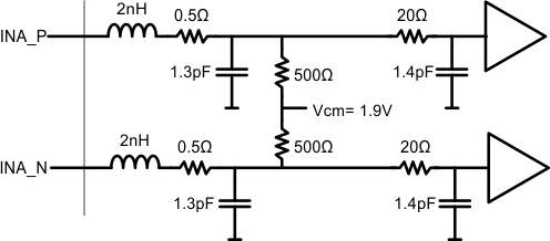 Figure 37. Equivalent Analog Input Circuit
8.3.4 Overrange Indication
The ADS5401 provides a fast overrange indication on the OVRA pins. The fast OVR is triggered if the input voltage exceeds the programmable overrange threshold and it gets presented after just 12 clock cycles enabling a quicker reaction to an overrange event. The OVR threshold can be configured using SPI register writes.
The input voltage level at which the overload is detected is referred to as the threshold and is programmable using the overrange threshold bits. The threshold at which fast OVR is triggered is (full-scale × [the decimal value of the FAST OVR THRESH bits] /16). After reset, the default value of the overrange threshold is set to 15 (decimal) which corresponds to a threshold of 0.56 dB below full scale (20 × log(15/16)).
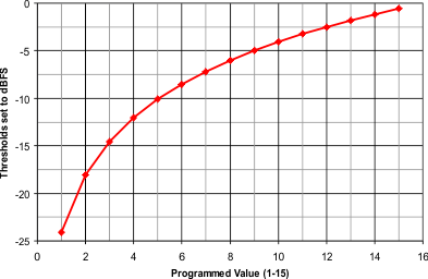 Figure 38. OVR Detection Threshold
8.3.5 Interleaving Correction
The two data converter channel consists of two interleaved ADCs each operating at half of the ADC sampling rate but 180º out of phase from each other. The front end track and hold circuitry is operating at the full ADC sampling rate which minimizes the timing mismatch between the two interleaved ADCs. In addition the ADS5401 is equipped with internal interleaving correction logic that can be enabled through SPI register write.
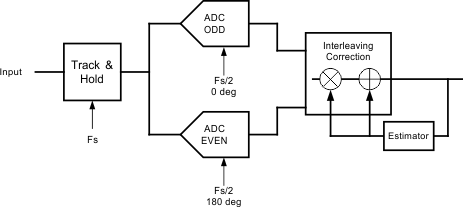 Figure 39. Interleaving Correction Circuit
The interleaving operation creates 2 distinct and interleaving products:
- Fs/2 – Fin: this spur is created by gain timing mismatch between the ADCs. Because internally the front end track and hold is operated at the full sampling rate, this component is greatly improved and mostly dependent on gain mismatch.
- Fs/2 Spur: due to offset mismatch between ADCs.
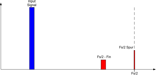 Figure 40. Interleaving Spur at Fs/2 due to Offset Mismatch
The auto correction loop can be enabled through SPI register write in address 0x01 and resetting the correction circuit in address 0x03. By default it is disabled for lowest possible power consumption.
The auto correction function yields best performance for input frequencies below 250 MHz.
8.3.6 Decimation Filter
There is an optional digital decimation filter in the data path as shown in Figure 41. The filter can be programmed as a lowpass or a highpass filter and the normalized frequency response of both filters is shown in Figure 42.
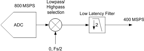 Figure 41. 2x Decimation Filter
The decimation filter response has a 0.1-dB pass band ripple with approximately 41% pass-band bandwidth. The stop-band attenuation is approximately 40 dB.
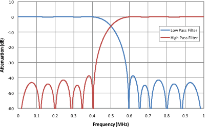 Figure 42. Decimation Filter Response
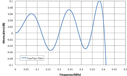 Figure 43. Decimation Filter Response
8.3.7 Multi Device Synchronization
The ADS5401 simplifies the synchronization of data from multiple ADCs in one common receiver. Upon receiving the initial SYNC input signal, the ADS5401 resets all the internal clocks and digital logic while also starting a SYNCOUT signal which operates on a 5-bit counter (32 clock cycles). Therefore by providing a common SYNC signal to multiple ADCs their output data can be synchronized as the SYNCOUT signal marks a specific sample with the same latency in all ADCs. The SYNCOUT signal then can be used in the receiving device to synchronize the FIFO pointers across the different input data streams. Thus the output data of multiple ADCs can be aligned properly even if there are different trace lengths between the different ADCs. By default ADS5401 is not configured for multi device synchronization. The ADC can be configured by setting the SYNCOUT enable bit (D2 config1) to 1 on all the ADCs.
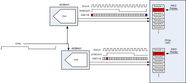 Figure 44. Multiple ADC Synchronization
The SYNC input signal should be a one time pulse to trigger the periodic 5-bit counter for SYNCOUT or a periodic signal repeating every 32 CLKIN clock cycles. It gets registered on the rising edge of the ADC input clock (CLKIN). Upon registering the initial rising edge of the SYNC signal, the internal clocks and logic get reset which results in invalid output data for 36 samples (1 complete sync cycle and 4 additional samples). The SYNCOUT signal starts with the next output clock (DACLK) rising edge and operates on a 5-bit counter. If a SYNCIN rising edge gets registered at a new position, the counter gets reset and SYNCOUT starts from the new position.
Because the ADS5401 output interface operates with a DDR clock, the synchronization can happen on the rising edge or falling edge sample. Synchronization on the falling edge sample will result in a half cycle clock stretch of DACLK. For convenience the SYNCOUT signal is available on the ChA output LVDS bus. When using decimation the SYNCOUT signal still operates on 32 clock cycles of CLKIN but since the output data is decimated by 2, only the first 18 samples should be discarded.
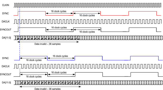 Figure 45. Multiple Device Synchronization Timing Diagram
8.4 Device Functional Modes
The ADS5401 has two main functional modes. The ADC can operate in Bypass mode in which sample rate and data-rate is the same or it can be programmed to operate in Decimate by 2x mode in which data rate is half of the sampling rate.
8.4.1 Power-Down Modes
The ADS5401 can be configured through SPI write (address x37) to a standby, light or deep sleep power mode which is controlled by the ENABLE pin. The sleep modes are active when the ENABLE pin goes low. Different internal functions stay powered up which results in different power consumption and wake up time between the two sleep modes.
Table 3. Power-Down Modes
| SLEEP MODE | WAKE-UP TIME | POWER CONSUMPTION AUTO CORRECTION DISABLED | POWER CONSUMPTION AUTO CORRECTION ENABLED |
|---|---|---|---|
| Complete Shut Down | 2.5 ms | 7mW | 7mW |
| Stand-by | 100µs | 7mW | 7mW |
| Deep Sleep | 20µs | 465mW | 530mW |
| Light Sleep | 2µs | 295mW | 360mW |
8.5 Programming
The serial interface (SIF) included in the ADS5401 is a simple 3 or 4 pin interface. In normal mode, 3 pins are used to communicate with the device. There is an enable (SDENB), a clock (SCLK) and a bidirectional IO port (SDIO). If the user would like to use the 4 pin interface one write must be implemented in the 3 pin mode to enable 4 pin communications. In this mode, the SDO pin becomes the dedicated output. The serial interface has an 8-bit address word and a 16-bit data word. The first rising edge of SCLK after SDENB goes low will latch the read/write bit. If a high is registered then a read is requested, if it is low then a write is requested. SDENB must be brought high again before another transfer can be requested. The signal diagram is shown below:
8.5.1 Device Initialization
After power up, TI recommends using the device through a hardware reset by applying a logic low pulse on the SRESETb pin (of width greater than 20ns), as shown in Figure 2. This resets all internal digital blocks (including SPI registers) to their default condition.
Recommended Device Initialization Sequence:
- Power up
- Reset ADS5401 using hardware reset.
- Apply clock and input signal.
- Set register 0x01 bit D15 to 1 (ChA Corr EN) to enable gain/offset correction circuit and other desired registers.
- Set register 0x03 bit D14 to 1 (Start Auto Corr ChA). This clears and resets the accumulator values in the DC and gain correction loop.
- Set register 0x03 bit D14 to 0 (Start Auto Corr ChA). This starts the DC and gain auto-correction loop.
8.5.2 Serial Register Write
The internal register of the ADS5401 can be programmed following these steps:
- Drive SDENB pin low
- Set the R/W bit to 0 (bit A7 of the 8 bit address)
- Initiate a serial interface cycle specifying the address of the register (A6 to A0) whose content has to be written
- Write 16bit data which is latched on the rising edge of SCLK
 Figure 46. Serial Register Write Timing Diagram
8.5.3 Serial Register Readout
The device includes a mode where the contents of the internal registers can be read back using the SDO/SDIO pins. This read-back mode may be useful as a diagnostic check to verify the serial interface communication between the external controller and the ADC.
- Drive SDENB pin low
- Set the RW bit (A7) to 1. This setting disables any further writes to the registers
- Initiate a serial interface cycle specifying the address of the register (A6 to A0) whose content has to be read.
- The device outputs the contents (D15 to D0) of the selected register on the SDO/SDIO pin
- The external controller can latch the contents at the SCLK rising edge.
- To enable register writes, reset the RW register bit to 0.
 Figure 47. Serial Register Read Timing Diagram
8.6 Register Maps
Table 4. Serial Register Map(1)
8.6.1 Register Name: Config0 - Address: 0×00, Default = 0×00
| Register Address | Register Data | |||||||||||||||
|---|---|---|---|---|---|---|---|---|---|---|---|---|---|---|---|---|
| A7-A0 in hex | D15 | D14 | D13 | D12 | D11 | D10 | D9 | D8 | D7 | D6 | D5 | D4 | D3 | D2 | D1 | D0 |
| 0 | 3-/4-wire SPI | Dec- ima- tion Filter EN |
0 | ChA High/ Low Pass | 0 | 0 | 0 | 0 | 0 | 0 | 0 | 0 | 0 | 0 | 0 | 0 |
| D15 | 3-/4-Wire SPI
Default 0 |
Enables 4-bit serial interface when set |
| 0 | 3-wire SPI is used with SDIO pin operating as bidirectional I/O port | |
| 1 | 4-wire SPI is used with SDIO pin operating as data input and SDO pin as data output port. | |
| D14 | Decimation Filter EN
Default 0 |
2x decimation filter is enabled when bit is set |
| 0 | Normal operation with data output at full sampling rate | |
| 1 | 2x decimation filter enabled | |
| D12 | ChA Highpass
or Lowpass Default 0 |
(Decimation filter must be enabled first: set bit D14) |
| 0 | Lowpass | |
| 1 | Highpass | |
8.6.2 Register Name: Config1 - Address: 0×01, Default = 0×00
| Register Address | Register Data | |||||||||||||||
|---|---|---|---|---|---|---|---|---|---|---|---|---|---|---|---|---|
| A7-A0 in hex | D15 | D14 | D13 | D12 | D11 | D10 | D9 | D8 | D7 | D6 | D5 | D4 | D3 | D2 | D1 | D0 |
| 1 | ChA Corr EN | 0 | 0 | 0 | 0 | 0 | 0 | 0 | 0 | 0 | 0 | 0 | Data Format | 0 | HP Mode1 | 0 |
| D15 | ChA Corr EN (should be enabled for maximum performance)
Default 0 |
|
| 0 | Auto correction disabled | |
| 1 | Auto correction enabled | |
| D3 | Data Format
Default 0 |
|
| 0 | Two's complement | |
| 1 | Offset Binary | |
| D2 | SYNCOUT Enable | |
| Default 0 | ||
| 1 | Must be set to 1 to enable SYNCOUT signal | |
| D1 | HP Mode 1
Default 0 |
|
| 1 | Must be set to 1 for optimum performance | |
8.6.3 Register Name: Config2 - Address: 0×02, Default = 0×780
| Register Address | Register Data | |||||||||||||||
|---|---|---|---|---|---|---|---|---|---|---|---|---|---|---|---|---|
| A7-A0 in hex | D15 | D14 | D13 | D12 | D11 | D10 | D9 | D8 | D7 | D6 | D5 | D4 | D3 | D2 | D1 | D0 |
| 2 | 0 | 0 | 0 | 0 | 0 | Over-range threshold | 0 | 0 | 0 | 0 | 0 | 0 | 0 | |||
| D10-D7 | Over-range threshold | The over-range detection is triggered 12 output clock cycles after the overload condition occurs. The threshold at which the OVR is triggered = 1.0V x [decimal value of <Over-range threshold>]/16. After power up or reset, the default value is 15 (decimal) which corresponds to a OVR threshold of 0.56dB below fullscale (20*log(15/16)). This OVR threshold is applicable to both channels. | ||
| Default 1111 | ||||
 Figure 51. OVR Detection Threshold
8.6.4 Register Name: 3 - Address: 0x03
| Register Address | Register Data | |||||||||||||||
|---|---|---|---|---|---|---|---|---|---|---|---|---|---|---|---|---|
| A7-A0 in hex | D15 | D14 | D13 | D12 | D11 | D10 | D9 | D8 | D7 | D6 | D5 | D4 | D3 | D2 | D1 | D0 |
| 3 | 0 | Start Auto Coff ChA | 0 | 0 | 1 | 0 | 1 | 1 | 0 | 0 | 0 | 1 | 1 | 0 | 0 | 0 |
| D14 | Start Auto Corr ChA
Default 1 |
Starts DC offset and Gain correction loop for ChA | |
| 0 | Starts the DC offset and Gain correction loops | ||
| 1 | Clears DC offset correction value to 0 and Gain correction value to 1 | ||
| D11, 9, 8, 4, 3 | Must be set to 1 for maximum performance Default 1 |
||
8.6.5 Register Name: E - Address: 0x0E
| Register Address | Register Data | |||||||||||||||
|---|---|---|---|---|---|---|---|---|---|---|---|---|---|---|---|---|
| A7-A0 in hex | D15 | D14 | D13 | D12 | D11 | D10 | D9 | D8 | D7 | D6 | D5 | D4 | D3 | D2 | D1 | D0 |
| E | Sync Select | 0 | 0 | |||||||||||||
| D15-D2 | Sync Select
Default 1010 1010 1010 10 |
Sync selection for the clock generator block (also need to see address 0x0F) | |
| 0000 0000 0000 00 | Sync is disabled | ||
| 0101 0101 0101 01 | Sync is set to one shot (one time synchronization only) | ||
| 1010 1010 1010 10 | Sync is derived from SYNC input pins | ||
| 1111 1111 1111 11 | not supported | ||
8.6.6 Register Name: F - Address: 0x0F
| Register Address | Register Data | |||||||||||||||
|---|---|---|---|---|---|---|---|---|---|---|---|---|---|---|---|---|
| A7-A0 in hex | D15 | D14 | D13 | D12 | D11 | D10 | D9 | D8 | D7 | D6 | D5 | D4 | D3 | D2 | D1 | D0 |
| F | Sync Select | 0 | 0 | 0 | 0 | 0 | VREF Sel | 0 | 0 | 0 | 0 | |||||
| D15-D12 | Sync Select
Default 1010 |
Sync selection for the clock generator block | |
| 0000 | Sync is disabled | ||
| 0101 | Sync is set to one shot (one time synchronization only) | ||
| 1010 | Sync is derived from SYNC input pins | ||
| 1111 | not supported | ||
| D6-D4 | VREF SEL
Default 000 |
Internal voltage reference selection | |
| 000 | 1.0V | ||
| 001 | 1.25V | ||
| 010 | 0.9V | ||
| 011 | 0.8V | ||
| 100 | 1.15V | ||
| Others | external reference | ||
8.6.7 Register Name: 2B - Address: 0x2B
| Register Address | Register Data | |||||||||||||||
|---|---|---|---|---|---|---|---|---|---|---|---|---|---|---|---|---|
| A7-A0 in hex | D15 | D14 | D13 | D12 | D11 | D10 | D9 | D8 | D7 | D6 | D5 | D4 | D3 | D2 | D1 | D0 |
| 2B | 0 | 0 | 0 | 0 | 0 | 0 | 0 | Temp Sensor | ||||||||
| D8-D0 | Temp Sensor | Internal temperature sensor value – read only |
8.6.8 Register Name: 2C - Address: 0x2C
| Register Address | Register Data | |||||||||||||||
|---|---|---|---|---|---|---|---|---|---|---|---|---|---|---|---|---|
| A7-A0 in hex | D15 | D14 | D13 | D12 | D11 | D10 | D9 | D8 | D7 | D6 | D5 | D4 | D3 | D2 | D1 | D0 |
| 2C | Reset | |||||||||||||||
| D15-D0 | Reset
Default 0000 |
This is a software reset to reset all SPI registers to their default value. Self clears to 0. | |
| 1101001011110000 | Perform software reset | ||
8.6.9 Register Name: 37 - Address: 0x37
| Register Address | Register Data | |||||||||||||||
|---|---|---|---|---|---|---|---|---|---|---|---|---|---|---|---|---|
| A7-A0 in hex | D15 | D14 | D13 | D12 | D11 | D10 | D9 | D8 | D7 | D6 | D5 | D4 | D3 | D2 | D1 | D0 |
| 37 | Sleep Modes | 0 | 0 | 0 | 0 | 0 | 0 | 0 | 0 | 0 | 0 | |||||
| D15-D10 | Sleep Modes
Default 00 |
Sleep mode selection which is controlled by the ENABLE pin. Sleep modes are active when ENABLE pin goes low. | |
| 000000 | Complete shut down | Wake up time 2.5 ms | |
| 100000 | Stand-by mode | Wake up time 100 µs | |
| 110000 | Deep sleep mode | Wake up time 20 µs | |
| 110101 | Light sleep mode | Wake up time 2 µs | |
8.6.10 Register Name: 38 - Address: 0x38
| Register Address | Register Data | |||||||||||||||
|---|---|---|---|---|---|---|---|---|---|---|---|---|---|---|---|---|
| A7-A0 in hex | D15 | D14 | D13 | D12 | D11 | D10 | D9 | D8 | D7 | D6 | D5 | D4 | D3 | D2 | D1 | D0 |
| 38 | HP Mode 2 | Bias EN | SYNC EN | LP Mode 1 | 1 | 1 | 1 | 1 | ||||||||
| D15-D7 | HP Mode 2
Default 111111111 |
||
| 1 | Set to 1 for normal operation | ||
| D6 | BIAS EN
Default 1 |
Enables internal fuse bias voltages – can be disabled after power up to save power. | |
| 0 | Internal bias powered down | ||
| 1 | Internal bias enabled | ||
| D5 | SYNC EN
Default 1 |
Enables the SYNC input buffer. | |
| 0 | SYNC input buffer disabled | ||
| 1 | SYNC input bffer enabled | ||
| D4 | LP Mode 1
Default 1 |
Low power mode 1 to disable internal unused input buffer. | |
| 0 | Internal input buffer disabled | ||
| 1 | Internal input buffer enabled | ||
| D3-D0 | Reads back 1 | ||
8.6.11 Register Name: 3A - Address: 0x3A
| Register Address | Register Data | |||||||||||||||
|---|---|---|---|---|---|---|---|---|---|---|---|---|---|---|---|---|
| A7-A0 in hex | D15 | D14 | D13 | D12 | D11 | D10 | D9 | D8 | D7 | D6 | D5 | D4 | D3 | D2 | D1 | D0 |
| 3A | LVDS Current Strength | LVDS SW | Internal LVDS Termination | 0 | 0 | 0 | 0 | DACLK EN | LP Mode 2 | 0 | OVRA EN | LP Mode 3 | ||||
| D15-D13 | LVDS Current Strength
Default 000 |
LVDS output current strength. | |||
| 000 | 2 mA | 100 | 3 mA | ||
| 001 | 2.25 mA | 101 | 3.25 mA | ||
| 010 | 2.5 mA | 110 | 3.5 mA | ||
| 011 | 2.75 mA | 111 | 3.75 mA | ||
| D12-D11 | LVDS SW
Default 01 |
LVDS driver internal switch setting – correct range must be set for setting in D15-D13 | |||
| 01 | 2 mA to 2.75 mA | ||||
| 11 | 3mA to 3.75mA | ||||
| D10-D9 | Internal LVDS Termination
Default 00 |
Internal termination | |||
| 00 | 2 kΩ | ||||
| 01 | 200 Ω | ||||
| 10 | 200 Ω | ||||
| 11 | 100 Ω | ||||
| D4 | DACLK EN
Default 1 |
Enable DACLK output buffer | |||
| 0 | DACLK output buffer powered down | ||||
| 1 | DACLK output buffer enabled | ||||
| D3 | LP Mode 2
Default 1 |
Low power mode to disable unused internal output buffer | |||
| 0 | Internal output buffer disabled | ||||
| 1 | internal output buffer enabled | ||||
| D1 | OVRA EN
Default 1 |
Enable OVRA output buffer | |||
| 0 | OVRA output buffer powered down | ||||
| 1 | OVRA output buffer enabled | ||||
| D0 | LP Mode 3
Default 1 |
Low power mode to disable unused internal output buffer | |||
| 0 | Internal output buffer disabled | ||||
| 1 | Internal output buffer enabled | ||||
8.6.12 Register Name: 66 - Address: 0x66
| Register Address | Register Data | |||||||||||||||
|---|---|---|---|---|---|---|---|---|---|---|---|---|---|---|---|---|
| A7-A0 in hex | D15 | D14 | D13 | D12 | D11 | D10 | D9 | D8 | D7 | D6 | D5 | D4 | D3 | D2 | D1 | D0 |
| 66 | LVDS Output Bus A EN | |||||||||||||||
| D15-D0 | LVDS Output Bus A EN
Default FFFF |
Individual LVDS output pin power down for channel A | |
| 0 | Output is powered down | ||
| 1 | Output is enabled | ||
| D15 | Pins N7, P7 (no connect pins) which are not used and should be powered down for power savings | ||
| D14 | Pins N6, P6 (no connect pins) which are not used and should be powered down for power savings | ||
| D13 | SYNCOUTP/N (pins P9, N9) | ||
| D12 | Pins P4, N4 (no connect pins) which are not used and should be powered down for power savings | ||
| D11-D0 | corresponds to DA11-DA0 | ||