SLAS918B December 2012 – April 2022 ADS54T01
PRODUCTION DATA
- 1 Features
- 2 Applications
- 3 Description
- 4 Revision History
- 5 Device Comparison
- 6 Pin Configuration and Functions
- 7 Specifications
-
8 Detailed Description
- 8.1 Overview
- 8.2 Functional Block Diagram
- 8.3
Feature Description
- 8.3.1 Test Pattern Output
- 8.3.2 Clock Inputs
- 8.3.3 SNR and Clock Jitter
- 8.3.4 Analog Inputs
- 8.3.5 Over-Range Indication
- 8.3.6 Interleaving Correction
- 8.3.7 High-Resolution Output Data
- 8.3.8 Low-Resolution Output Data
- 8.3.9 Full Speed – 7 Bit
- 8.3.10 Decimated Low-Resolution Output Data
- 8.3.11 Multi Device Synchronization
- 8.4 Device Functional Modes
- 8.5 Programming
- 8.6 Register Maps
- 9 Power Supply Recommendations
- 10Device and Documentation Support
- 11Mechanical, Packaging, and Orderable Information
Package Options
Mechanical Data (Package|Pins)
- ZAY|196
Thermal pad, mechanical data (Package|Pins)
Orderable Information
8.3.4 Analog Inputs
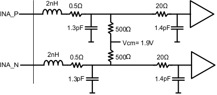
The ADS54T01 analog signal input is designed to be driven differentially. The analog input pins have internal analog buffers that drive the sampling circuit. As a result of the analog buffer, the input pins present a high impedance input across a very wide frequency range to the external driving source which enables great flexibility in the external analog filter design as well as excellent 50 Ω matching for RF applications. The buffer also helps isolate the external driving circuit from the internal switching currents of the sampling circuit which results in a more constant SFDR performance across input frequencies.
The common-mode voltage of the signal inputs is internally biased to 1.9 V using 500-Ω resistors which allows for AC coupling of the input drive network. Each input pin (INP, INM) must swing symmetrically between (VCM + 0.25 V) and (VCM – 0.25 V), resulting in a 1.0 Vpp (default) differential input swing. The input sampling circuit has a 3-dB bandwidth that extends up to 1.2 GHz.
 Figure 8-5 Analog Input Internal Circuitry