SBAS682D November 2014 – December 2015 ADS7044
PRODUCTION DATA.
- 1 Features
- 2 Applications
- 3 Description
- 4 Revision History
- 5 Pin Configuration and Functions
- 6 Specifications
- 7 Parameter Measurement Information
- 8 Detailed Description
- 9 Application and Implementation
- 10Power-Supply Recommendations
- 11Layout
- 12Device and Documentation Support
- 13Mechanical, Packaging, and Orderable Information
Package Options
Refer to the PDF data sheet for device specific package drawings
Mechanical Data (Package|Pins)
- DCU|8
- RUG|8
Thermal pad, mechanical data (Package|Pins)
Orderable Information
10 Power-Supply Recommendations
10.1 AVDD and DVDD Supply Recommendations
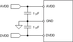
The device has two separate power supplies: AVDD and DVDD. The device operates on AVDD; DVDD is used for the interface circuits. AVDD and DVDD can be independently set to any value within the permissible ranges. The AVDD supply also defines the full-scale input range of the device. Decouple the AVDD and DVDD pins individually with 1-µF ceramic decoupling capacitors, as shown in Figure 45. The minimum capacitor value required for AVDD and DVDD is 200 nF and 20 nF, respectively. If both supplies are powered from the same source, a minimum capacitor value of 220 nF is required for decoupling.
 Figure 45. Power-Supply Decoupling
10.2 Estimating Digital Power Consumption
The current consumption from the DVDD supply depends on the DVDD voltage, load capacitance on the SDO line, and the output code. The load capacitance on the SDO line is charged by the current from the SDO pin on every rising edge of the data output and is discharged on every falling edge of the data output. The current consumed by the device from the DVDD supply can be calculated by Equation 4:
where
- C = Load capacitance on the SDO line,
- V = DVDD supply voltage, and
- f = Number of transitions on the SDO output.
The number of transitions on the SDO output depends on the output code, and thus changes with the analog input. The maximum value of f occurs when data output on the SDO change on every SCLK. SDO changing on every SCLK results in an output code of AAAh or 555h. For an output code of AAAh or 555h at a 1-MSPS throughput, the frequency of transitions on the SDO output is 6 MHz.
To keep the current consumption at the lowest possible value, the DVDD supply must be kept at the lowest permissible value and the capacitance on the SDO line must be kept as low as possible.
10.3 Optimizing Power Consumed by the Device
- Keep the analog supply voltage (AVDD) as per the analog input full-scale range (FSR) requirement.
- Keep the digital supply voltage (DVDD) at the lowest permissible value.
- Reduce the load capacitance on the SDO output.
- Run the device at optimum throughput. Power consumption reduces with throughput.