SLAS468A June 2005 – August 2016 ADS7887 , ADS7888
PRODUCTION DATA.
- 1 Features
- 2 Applications
- 3 Description
- 4 Revision History
- 5 Companion Products
- 6 Device Comparison
- 7 Pin Configuration and Functions
- 8 Specifications
- 9 Detailed Description
- 10Application and Implementation
- 11Power Supply Recommendations
- 12Layout
- 13Device and Documentation Support
- 14Mechanical, Packaging, and Orderable Information
Package Options
Mechanical Data (Package|Pins)
Thermal pad, mechanical data (Package|Pins)
- DCK|6
Orderable Information
10 Application and Implementation
NOTE
Information in the following applications sections is not part of the TI component specification, and TI does not warrant its accuracy or completeness. TI’s customers are responsible for determining suitability of components for their purposes. Customers should validate and test their design implementation to confirm system functionality.
10.1 Application Information
The primary circuits required to maximize the performance of a high-precision, the successive approximation register (SAR) and analog-to-digital converter (ADC), are the input driver and the reference driver circuits. This section details some general principles for designing the input driver circuit, references the driver circuit, and provides some application circuits designed for the ADS7887 and ADS7888.
10.2 Typical Application
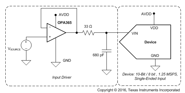
 Figure 37. Typical Data Acquisition (DAQ) Circuit: Single-Supply DAQ
10.2.1 Design Requirements
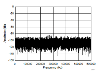
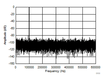
The goal of this application is to design a single-supply digital acquisition (DAQ) circuit based on the ADS7887 with SNR greater than 61 dB and THD less than –84 dB for input frequencies of 2 kHz to 100 kHz at a throughput of 1.25 MSPS.
10.2.2 Detailed Design Procedure
To achieve a SINAD of 61 dB, the operational amplifier must have high bandwidth to settle the input signal within the acquisition time of the ADC. The operational amplifier must have low noise to keep the total system noise below 20% of the input-referred noise of the ADC. For the application circuit shown in Figure 37, OPA365 is selected for its high bandwidth (50 MHz) and low noise (4.5 nV√Hz).
The reference voltage for the ADS7887 and ADS7888 A/D converters are derived from the supply voltage internally. The supply to these converters must be driven with a low impedance source and must be decoupled to the ground. To drive supply pin of ADS7887 ultra low noise fast transient response low dropout voltage regulator TPS73201 is selected. Alternatively one can drive supply pin with low impedance voltage reference similar to REF3030.
For a step-by-step design procedure for low power, small form factor digital acquisition (DAQ) circuit based on similar SAR ADCs refer to TI Precision Design, Three 12-Bit Data Acquisition Reference Designs Optimized for Low Power and Ultra-Small Form Factor.
10.2.3 Application Curves

| SNR: 61.9 dB | THD: –86.8 dB | SINAD: 61.3 dB |

| SNR: 61.8 dB | THD: –85.1 dB | SINAD: 61.5 dB |