SBAS652A May 2014 – August 2014 ADS7950-Q1 , ADS7951-Q1 , ADS7952-Q1 , ADS7953-Q1 , ADS7954-Q1 , ADS7956-Q1 , ADS7957-Q1 , ADS7958-Q1 , ADS7959-Q1 , ADS7960-Q1 , ADS7961-Q1
PRODUCTION DATA.
- 1 Features
- 2 Applications
- 3 Description
- 4 Revision History
- 5 Device Comparison Table
- 6 Pin Configurations and Functions
-
7 Specifications
- 7.1 Absolute Maximum Ratings
- 7.2 Handling Ratings
- 7.3 Recommended Operating Conditions
- 7.4 Thermal Information
- 7.5 Electrical Characteristics: ADS7950-Q1, ADS7951-Q1, ADS7952-Q1, ADS7953-Q1
- 7.6 Electrical Characteristics: ADS7954-Q1, ADS7956-Q1, ADS7957-Q1
- 7.7 Electrical Characteristics: ADS7958-Q1, ADS7959-Q1, ADS7960-Q1, ADS7961-Q1
- 7.8 Timing Requirements
- 7.9 Typical Characteristics (All ADS79xx-Q1 Family Devices)
- 7.10 Typical Characteristics (12-Bit Devices Only)
- 8 Detailed Description
- 9 Application and Implementation
- 10Power-Supply Recommendations
- 11Layout
- 12Device and Documentation Support
- 13Mechanical, Packaging, and Orderable Information
Package Options
Mechanical Data (Package|Pins)
- DBT|30
Thermal pad, mechanical data (Package|Pins)
Orderable Information
9 Application and Implementation
9.1 Application Information
In general applications, when the internal multiplexer is updated, the previously converted channel charge is stored in the 15-pF internal input capacitance that disturbs the voltage at the newly selected channel. This disturbance is expected to settle to 1 LSB during sampling (acquisition) time to avoid degrading converter performance. The initial absolute disturbance error at the channel input must be less than 0.5 V to prevent source current saturation or slewing that causes significantly long settling times. Fortunately, significantly reducing disturbance error is easy to accomplish by simply placing a large enough capacitor at the input of each channel. Specifically, with a 150-pF capacitor, instantaneous charge distribution keeps disturbance error below 0.46 V because the internal input capacitance can only hold up to 75 pC (or 5 V × 15 pF). The remaining error must be corrected by the voltage source at each input, with impedance low enough to settle within 1 LSB. The following application examples explain the considerations for the input source impedance (RSOURCE).
9.2 Typical Applications
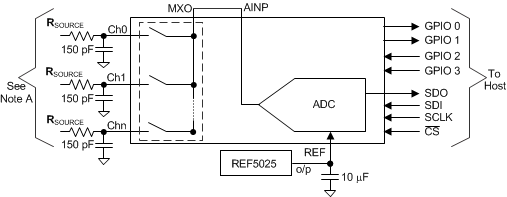
9.2.1 Unbuffered Multiplexer Output (MXO)
This application is the most typical application, but requires the lowest RSOURCE for good performance. In this configuration, the 2xREF range allows larger source impedance than the 1xREF range because the 1xREF range LSB size is smaller, thus making it more sensitive to settling error.
9.2.1.1 Design Requirements
The design is optimized to show the input source impedance (RSOURCE) between the 100 Ω to 10,000 Ω required to meet the 1-LSB settling at 12-bit, 10-bit, and 8-bit resolutions at different throughput in 1xREF (2.5-V) and 2xREF (5-V) input ranges.
9.2.1.2 Detailed Design Procedure
Although the required input source impedance can be estimated assuming a 0.5-V initial error and exponential recovery during sampling (acquisition) time, this estimation over-simplifies the complex interaction between the converter and source, thus yielding inaccurate estimates. Thus, this design uses an iterative approach with the converter itself to provide reliable impedance values.
To determine the actual maximum source impedance for a particular resolution and sampling rate, two subsequent channels are set at least 95% of the full-scale range apart. With a 1xREF range and 2.5 Vref, the channel difference is at least 2.375 V. With 2xREF and 2.5 Vref, the difference is at least 4.75 V. With a source impedance between 100 Ω to 10,000 Ω, the conversion runs at a constant rate and a channel update is issued that captures the first couple samples after the update. This process is repeated at least 100 times to remove any noise and to show a clear settling error. The first sample after the channel update is then compared against the second one. If the first and second samples are more than 1 LSB apart, throughput rate is reduced until the settling error becomes 1 LSB, which then sets the maximum throughput for the selected impedance. The whole process is repeated for nine different impedances between 100 Ω to 10,000 Ω.
9.2.1.3 Application Curves
These curves show the RSOURCE for an unbuffered MXO.
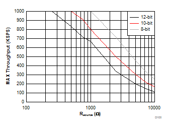 Figure 59. 2xREF Input Range Settling without an MXO Buffer
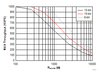 Figure 60. 1xREF Input Range Settling without an MXO Buffer
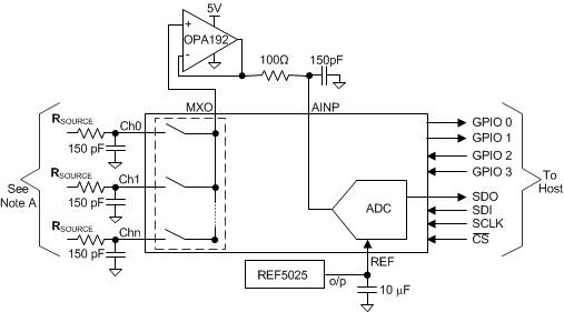
9.2.2 OPA192 Buffered Multiplexer Output (MXO)
The use of a buffer relaxes the RSOURCE requirements to an extent. Charge from the sample-and-hold capacitor no longer dominates as a residual charge from a previous channel. Although having good performance is possible with a larger impedance using the OPA192, the output capacitance of the MXO also holds the previous channel charge and cannot be isolated, which limits how large the input impedance can finally be for good performance. In this configuration, the 1xREF range allows slightly higher impedance because the OPA192
(20 V/µs) slews approximately 2.5 V in contrast to the 2xREF range that requires the OPA192 to slew approximately 5 V.
9.2.2.1 Design Requirements
The design is optimized to show the input source impedance (RSOURCE) between the 100 Ω to 10,000 Ω required to meet a 1-LSB settling at 12-bit, 10-bit, and 8-bit resolutions at different throughput in 1xREF (2.5 V) and 2xREF (5 V) input ranges.
9.2.2.2 Detailed Design Procedure
The design procedure is similar to the unbuffered-MXO application, but includes an operation amplifier in unity gain as a buffer. The most important parameter for multiplexer buffering is slew rate. The amplifier must finish slewing before the start of sampling (acquisition) to keep the buffer operating in small-signal mode during sampling (acquisition) time. Also, between the buffer output and converter input (INP), there must be a capacitor large enough to keep the buffer in small-signal operation during sampling (acquisition) time. Because 150 pF is large enough to protect the buffer form hold charge from internal capacitors, this value selected along with the lowest impedance that allows the op amp to remain stable.
The converter allows the MXO to settle approximately 600 ns before sampling. During this time, the buffer slews and then enters small-signal operation. For a 5-V step change, slew rate stays constant during the first 4 V. The last 1 V includes a transition from slewing and non-slewing. Thus, the buffer cannot be assumed to keep a constant slew during the 600 ns available for MXO settling. Assuming that the last 1-V slew is reduced to half is recommended. For this reason, slew is 10 V/µs or (5 Vref + 1 V) / 0.6 µs to account for the 1-V slow slew. The OPA192 has a 20-V/us slew, and is capable of driving 150 pF with more than a 50° phase margin with a 50-Ω or 100-Ω Riso, making the OPA192 an ideal selection for the ADS79xx-Q1 family of converters.
9.2.2.3 Application Curves
These curves show the RSOURCE for an OPA192 buffered MXO.
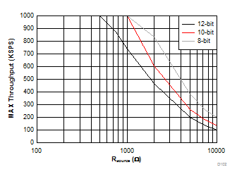 Figure 62. 2xREF Input Range Settling with an OPA192 MXO Buffer
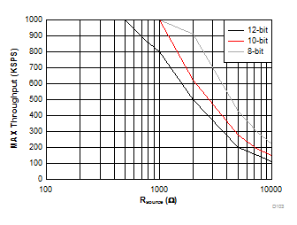 Figure 63. 1xREF Input Range Settling with an OPA192 MXO Buffer
9.3 Do's and Don'ts
- Use capacitors to decouple the dynamic current transients at each pins, including reference, supply, and input signal.
- Do not place capacitors on the MXO pin. This placement causes issues with the signal settling when the multiplexer changes channels.
- Depending on the PCB layout, there can be parasitic inductance on the SCLK trace that causes ringing. To minimize ringing, do not place a capacitor at the SCLK pin. Instead, place a small resistor in series with the SCLK pin to slow down the clock edges.