SBAS761A February   2020  – February 2020 ADS8355

PRODUCTION DATA.  

  1. Features
  2. Applications
  3. Description
    1.     Device Images
      1.      Typical Block Diagram
  4. Revision History
  5. Pin Configuration and Functions
    1.     Pin Functions
  6. Specifications
    1. 6.1      Absolute Maximum Ratings
    2. 6.2      ESD Ratings
    3. 6.3      Recommended Operating Conditions
    4. 6.4      Thermal Information
    5. 6.5      Electrical Characteristics
    6. Table 1. Timing Requirements
    7. Table 2. Switching Characteristics
    8. 6.6      Typical Characteristics
  7. Detailed Description
    1. 7.1 Overview
    2. 7.2 Functional Block Diagram
    3. 7.3 Feature Description
      1. 7.3.1 Reference
      2. 7.3.2 Analog Inputs
        1. 7.3.2.1 Analog Input: Full-Scale Range Selection
        2. 7.3.2.2 Analog Input: Single-Ended and Pseudo-Differential Configurations
      3. 7.3.3 Transfer Function
    4. 7.4 Device Functional Modes
      1. 7.4.1 Conversion Data Read: Dual-SDO Mode (Default)
      2. 7.4.2 Conversion Data Read: Single-SDO Mode
      3. 7.4.3 Low-Power Modes
        1. 7.4.3.1 STANDBY Mode
        2. 7.4.3.2 PD (Power-Down) Mode
    5. 7.5 Programming
      1. 7.5.1 Register Read/Write Operation
    6. 7.6 Register Map
      1. 7.6.1 ADS8355 Registers
        1. 7.6.1.1  PD_STANDBY Register (Offset = 4h) [reset = 0h]
          1. Table 9. PD_STANDBY Register Field Descriptions
        2. 7.6.1.2  PD_KEY Register (Offset = 5h) [reset = 0h]
          1. Table 10. PD_KEY Register Field Descriptions
        3. 7.6.1.3  SDO_CTRL Register (Offset = Dh) [reset = 0h]
          1. Table 11. SDO_CTRL Register Field Descriptions
        4. 7.6.1.4  DATA_OUT_CTRL Register (Offset = 11h) [reset = 0h]
          1. Table 12. DATA_OUT_CTRL Register Field Descriptions
        5. 7.6.1.5  REF_SEL Register (Offset = 20h) [reset = 0h]
          1. Table 13. REF_SEL Register Field Descriptions
        6. 7.6.1.6  REFDAC_A_LSB Register (Offset = 24h) [reset = 0h]
          1. Table 14. REFDAC_A_LSB Register Field Descriptions
        7. 7.6.1.7  REFDAC_A_MSB Register (Offset = 25h) [reset = 0h]
          1. Table 15. REFDAC_A_MSB Register Field Descriptions
        8. 7.6.1.8  REFDAC_B_LSB Register (Offset = 26h) [reset = 0h]
          1. Table 16. REFDAC_B_LSB Register Field Descriptions
        9. 7.6.1.9  REFDAC_B_MSB Register (Offset = 27h) [reset = 0h]
          1. Table 17. REFDAC_B_MSB Register Field Descriptions
        10. 7.6.1.10 INPUT_CONFIG Register (Offset = 28h) [reset = 0h]
          1. Table 18. INPUT_CONFIG Register Field Descriptions
  8. Application and Implementation
    1. 8.1 Application Information
      1. 8.1.1 Input Amplifier Selection
      2. 8.1.2 Charge Kickback Filter
    2. 8.2 Typical Application
      1. 8.2.1 Design Requirements
      2. 8.2.2 Detailed Design Procedure
      3. 8.2.3 Application Curve
  9. Power Supply Recommendations
  10. 10Layout
    1. 10.1 Layout Guidelines
    2. 10.2 Layout Example
  11. 11Device and Documentation Support
    1. 11.1 Device Support
      1. 11.1.1 Development Support
    2. 11.2 Documentation Support
      1. 11.2.1 Related Documentation
    3. 11.3 Receiving Notification of Documentation Updates
    4. 11.4 Community Resources
    5. 11.5 Trademarks
    6. 11.6 Electrostatic Discharge Caution
    7. 11.7 Glossary
  12. 12Mechanical, Packaging, and Orderable Information

Package Options

Mechanical Data (Package|Pins)
Thermal pad, mechanical data (Package|Pins)
Orderable Information

Application Curve

To minimize external components and to maximize the dynamic range of the ADC, the device is configured to operate with an internal reference (REF_SEL register, INT_EXT bit = 1) and a 2 × VREF_x input full-scale range (INPUT_CONFIG register, RANGE_SEL bit = 1). The REFDAC_x registers are programmed to 0x1FFh to program the internal reference to 2.5 V.

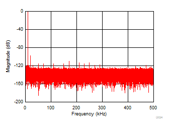
Figure 46 shows the FFT plot and test result obtained with the ADS8355 operating at full throughput with a dual-SDO interface and the circuit configuration of Figure 44.
ADS8355 D024.gif
SNR = 86.38 dB, THD = –97.24 dB, fIN = 10 kHz
Figure 46. The ADS8355 in Dual-SDO Interface Mode