SBAS797 February 2017 AMC1305L25-Q1 , AMC1305M05-Q1 , AMC1305M25-Q1
PRODUCTION DATA.
- 1 Features
- 2 Applications
- 3 Description
- 4 Revision History
- 5 Device Comparison Table
- 6 Pin Configurations and Functions
-
7 Specifications
- 7.1 Absolute Maximum Ratings
- 7.2 ESD Ratings
- 7.3 Recommended Operating Conditions
- 7.4 Thermal Information
- 7.5 Power Ratings
- 7.6 Insulation Specifications
- 7.7 Safety-Related Certifications
- 7.8 Safety Limiting Values
- 7.9 Electrical Characteristics: AMC1305M05-Q1
- 7.10 Electrical Characteristics: AMC1305x25-Q1
- 7.11 Switching Characteristics
- 7.12 Insulation Characteristics Curves
- 7.13 Typical Characteristics
- 8 Detailed Description
- 9 Application and Implementation
- 10Power-Supply Recommendations
- 11Layout
- 12Device and Documentation Support
- 13Mechanical, Packaging, and Orderable Information
Package Options
Mechanical Data (Package|Pins)
- DW|16
Thermal pad, mechanical data (Package|Pins)
- DW|16
Orderable Information
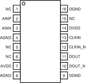
6 Pin Configurations and Functions
DW Package
16-Pin SOIC
Top View

LVDS Versions (AMC1305L25-Q1)
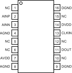
DW Package
16-Pin SOIC
Top View

CMOS Versions (AMC1305Mx-Q1)
Pin Functions
| PIN | I/O | DESCRIPTION | |
|---|---|---|---|
| NAME | NO. | ||
| AGND | 4 | — | This pin is internally connected to pin 8 and can be left unconnected or tied to high-side ground |
| 8 | — | High-side ground reference | |
| AINN | 3 | I | Inverting analog input |
| AINP | 2 | I | Noninverting analog input |
| AVDD | 7 | — | High-side power supply, 4.5 V to 5.5 V. See the Power-Supply Recommendations section for decoupling recommendations. |
| CLKIN | 13 | I | Modulator clock input, 5 MHz to 20.1 MHz |
| CLKIN_N | 12 | I | AMC1305L25-Q1 only: inverted modulator clock input |
| DGND | 9, 16 | — | Controller-side ground reference |
| DOUT | 11 | O | Modulator data output |
| DOUT_N | 10 | O | AMC1305L25-Q1 only: inverted modulator data output |
| DVDD | 14 | — | Controller-side power supply, 3.0 to 5.5 V |
| NC | 1 | — | This pin can be connected to AVDD or can be left unconnected |
| 5 | — | This pin can be left unconnected or tied to AGND only | |
| 6, 10, 12 | — | These pins have no internal connection (pins 10 and 12 on the AMC1305Mx-Q1 only). | |
| 15 | — | This pin can be left unconnected or tied to DVDD only | |