SLUSDU0A september 2019 – august 2023 BQ21061
PRODUCTION DATA
- 1
- 1 Features
- 2 Applications
- 3 Description
- 4 Revision History
- 5 Pin Configuration and Functions
- 6 Specifications
-
7 Detailed Description
- 7.1 Overview
- 7.2 Functional Block Diagram
- 7.3
Feature Description
- 7.3.1 Linear Charger and Power Path
- 7.3.2 Protection Mechanisms
- 7.3.3 VDD LDO
- 7.3.4 Load Switch/LDO Output and Control
- 7.3.5 PMID Power Control
- 7.3.6 System Voltage (PMID) Regulation
- 7.3.7 MR Wake and Reset Input
- 7.3.8 14-Second Watchdog for HW Reset
- 7.3.9 Faults Conditions and Interrupts ( INT)
- 7.3.10 Power Good ( PG) Pin
- 7.3.11 External NTC Monitoring (TS)
- 7.3.12 I2C Interface
- 7.4 Device Functional Modes
- 7.5 Register Map
- 8 Application and Implementation
- 9 Power Supply Recommendations
- 10Layout
- 11Device and Documentation Support
- 12Mechanical, Packaging, and Orderable Information
Package Options
Mechanical Data (Package|Pins)
- YFP|20
Thermal pad, mechanical data (Package|Pins)
Orderable Information
5 Pin Configuration and Functions
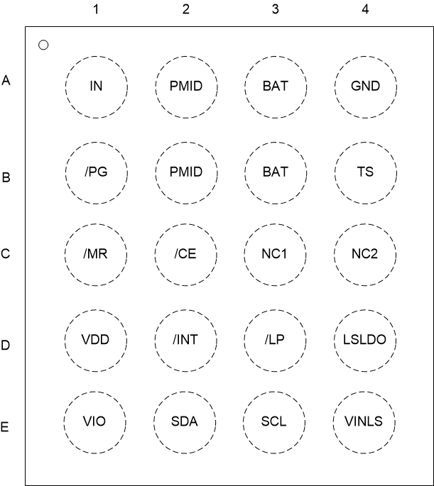
 Figure 5-1 YFP Package20-Pin DSBGATop View
Table 5-1 Pin Functions
| PIN | I/O | DESCRIPTION | |
|---|---|---|---|
| NAME | NO. | ||
| IN | A1 | I | DC Input Power Supply. IN is connected to the external DC supply. Bypass IN to GND with at least 1-µF of capacitance using a ceramic capacitor. |
| PMID | A2, B2 | I/O | Regulated System Output. Connect 22-µF capacitor from PMID to GND as close to the PMID and GND pins as possible. If operating in VIN Pass-Through Mode (PMID_REG = 111) a lower capacitor value may be used (at least 3-µF of ceramic capacitance with DC bias de-rating). |
| GND | A4 | PWR | Ground connection. Connect to the ground plane of the circuit. |
| VDD | D1 | O | Digital supply LDO. Connect a 2.2-µF from this pin to ground. |
| CE | C2 | I | Charge Enable. Drive CE low or leave disconnected to enable charging when VIN is valid. CE is pulled low internally with 900-kΩ resistor. |
| SCL | E3 | I/O | I2C Interface Clock. Connect SCL to the logic rail through a 10-kΩ resistor. |
| SDA | E2 | I | I2C Interface Data. Connect SDA to the logic rail through a 10-kΩ resistor. |
| LP | D3 | I | Low Power Mode Enable. Drive this pin low to set the device in low power mode when powered by the battery. This pin must be driven high to allow I2C communication when VIN is not present. LP is pulled low internally with 900-kΩ resistor. This pin has no effect when VIN is present. |
| INT | D2 | O | INT is an open-drain output that signals fault interrupts. When a fault occurs, a 128-µs pulse is sent out as an interrupt for the host. |
| MR | C1 | I | Manual Reset Input. MR is a general purpose input used to reset the device or to wake it up from Ship Mode. MR has in internal 125-kΩ pull-up resistor to BAT. |
| LS/LDO | D4 | O | Load Switch or LDO output. Connect 2.2 µF of ceramic capacitance to this pin to assure stability. Be sure to account for capacitance bias voltage derating when selecting the capacitor. If LDO is not used, short to VINLS |
| VINLS | E4 | I | Input to the Load Switch / LDO output. Connect at least 1 µF of ceramic capacitance from this pin to ground. |
| BAT | A3, B3 | I/O | Battery Connection. Connect to the positive terminal of the battery. Bypass BAT to GND with at least 1 µF of ceramic capacitance. |
| TS | B4 | I | Battery Pack NTC Monitor. Connect TS to a 10-kΩ NTC thermistor in parallel to a 10-kΩ resistor. If TS function is not to be used connect a 5-kΩ resistor from TS to ground. |
| PG | B1 | O | Open-drain Power Good status indication output. The PG pin can also be configured as a general purpose open drain output or level shifter version of MR. |
| VIO | E1 | I | System IO supply. Connect to system IO supply to allow level shifting of input signals (SDA, SCL, LP and CE) to the device internal digital domain. Connect to VDD when external IO supply is not available. |
| NC1 | C3 | I | No Connect. Connect to ground if possible for better thermal dissipation or leave floating. Do not connect to a any voltage source or signal to avoid higher quiescent current. |
| NC2 | C4 | I | No Connect. Connect to ground if possible for better thermal dissipation. May be shorted to /LP for easier routing as long as Absolute Maximum Rating requirements are met.. |