SLUSCM1A October 2017 – December 2017
PRODUCTION DATA.
- 1 Features
- 2 Applications
- 3 Description
- 4 Revision History
- 5 Description (continued)
- 6 Device Comparison Table
- 7 Pin Configuration and Functions
- 8 Specifications
- 9 Detailed Description
- 10Application and Implementation
- 11Power Supply Recommendations
- 12Layout
- 13Device and Documentation Support
- 14Mechanical, Packaging, and Orderable Information
Package Options
Mechanical Data (Package|Pins)
- RGT|16
Thermal pad, mechanical data (Package|Pins)
- RGT|16
Orderable Information
9 Detailed Description
9.1 Overview
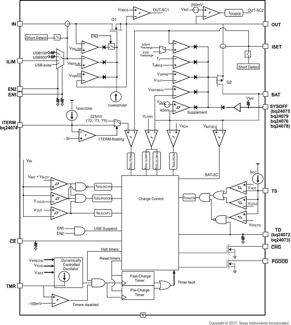
The bq2407x devices are integrated Li-Ion linear chargers and system power path management devices targeted at space-limited portable applications. The device powers the system while simultaneously and independently charging the battery. This feature reduces the number of charge and discharge cycles on the battery, allows for proper charge termination and enables the system to run with a defective or absent battery pack. This feature also allows instant system turn-on even with a totally discharged battery. The input power source for charging the battery and running the system can be an AC adapter or a USB port. The devices feature Dynamic Power Path Management (DPPM), which shares the source current between the system and battery charging, and automatically reduces the charging current if the system load increases. When charging from a USB port, the input dynamic power management (VIN-DPM) circuit reduces the input current if the input voltage falls below a threshold, thus preventing the USB port from crashing. The power-path architecture also permits the battery to supplement the system current requirements when the adapter cannot deliver the peak system currents.
9.2 Functional Block Diagram
9.3 Feature Description
9.3.1 Undervoltage Lockout (UVLO)
The bq2407x family remains in power down mode when the input voltage at the IN pin is below the undervoltage threshold (UVLO).
During the power down mode the host commands at the control inputs (CE, EN1 and EN2) are ignored. The Q1 FET connected between IN and OUT pins is off, and the status outputs CHG and PGOOD are high impedance. The Q2 FET that connects BAT to OUT is ON. (If SYSOFF is high, Q2 is off). During power down mode, the VOUT(SC2) circuitry is active and monitors for overload conditions on OUT.
9.3.2 Power On
When VIN exceeds the UVLO threshold, the bq2407x powers up. While VIN is below VBAT + VIN(DT), the host commands at the control inputs (CE, EN1 and EN2) are ignored. The Q1 FET connected between IN and OUT pins is off, and the status outputs CHG and PGOOD are high impedance. The Q2 FET that connects BAT to OUT is ON. (If SYSOFF is high, Q2 is off). During this mode, the VOUT(SC2) circuitry is active and monitors for overload conditions on OUT.
Once VIN rises above VBAT + VIN(DT), PGOOD is driven low to indicate the valid power status and the CE, EN1, and EN2 inputs are read. The device enters standby mode if (EN1 = EN2 = HI) or if an input overvoltage condition occurs. In standby mode, Q1 is OFF and Q2 is ON so OUT is connected to the battery input. (If SYSOFF is high, FET Q2 is off). During this mode, the VOUT(SC2) circuitry is active and monitors for overload conditions on OUT.
When the input voltage at IN is within the valid range: VIN > UVLO AND VIN > VBAT + VIN(DT) AND VIN < VOVP, and the EN1 and EN2 pins indicate that the USB suspend mode is not enabled [(EN1, EN2) ≠ (HI, HI)] all internal timers and other circuit blocks are activated. The device then checks for short-circuits at the ISET and ILIM pins. If no short conditions exists, the device switches on the input FET Q1 with a 100mA current limit to checks for a short circuit at OUT. When VOUT is above VO(SC1), the FET Q1 switches to the current limit threshold set by EN1, EN2 and RILIM and the device enters into the normal operation. During normal operation, the system is powered by the input source (Q1 is regulating), and the device continuously monitors the status of CE, EN1 and EN2 as well as the input voltage conditions.
 Figure 13. Startup Flow Diagram
9.3.3 Overvoltage Protection (OVP)
The bq2407x accepts inputs up to 28 V without damage. Additionally, an overvoltage protection (OVP) circuit is implemented that shuts off the internal LDO and discontinues charging when VIN > VOVP for a period long than tDGL(OVP). When in OVP, the system output (OUT) is connected to the battery and PGOOD is high impedance. Once the OVP condition is removed, a new power on sequence starts (see Power On). The safety timers are reset and a new charge cycle will be indicated by the CHG output.
9.3.4 Dynamic Power-Path Management
The bq2407x features an OUT output that powers the external load connected to the battery. This output is active whenever a source is connected to IN or BAT. The following sections discuss the behavior of OUT with a source connected to IN to charge the battery and a battery source only.
9.3.4.1 Input Source Connected (ADAPTER or USB)
With a source connected, the dynamic power-path management (DPPM) circuitry of the bq2407x monitors the input current continuously. For the bq24076/78, OUT is regulated to 210 mV above the voltage at BAT. When the BAT voltage falls below 3.2 V, OUT is clamped to 3.41 V. This allows for proper startup of the system load even with a discharged battery. The current into IN is shared between charging the battery and powering the system load at OUT. The bq2407x has internal selectable current limits of 100 mA (USB100) and 500 mA (USB500) for charging from USB ports, as well as a resistor-programmable input current limit.
The bq2407x is USB IF compliant for the inrush current testing. The USB specification allows up to 10 μF to be hard started, which establishes 50 μC as the maximum inrush charge value when exceeding 100 mA. The input current limit for the bq2407x prevents the input current from exceeding this limit, even with system capacitances greater than 10 μF. The input capacitance to the device must be selected small enough to prevent a violation (<10 μF), as this current is not limited. Figure 14 demonstrates the start-up of the bq2407x and compares it to the USB-IF specification.
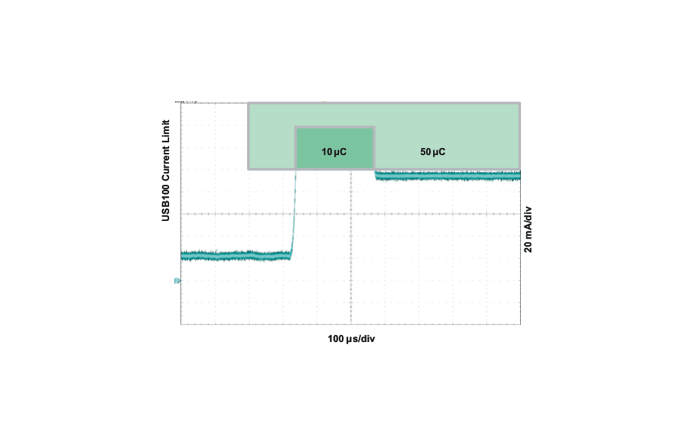 Figure 14. USB-IF Inrush Current Test
The input current limit selection is controlled by the state of the EN1 and EN2 pins as shown in the EN1/EN2 Settings table in Pin Configuration and Functions. When using the resistor-programmable current limit, the input current limit is set by the value of the resistor connected from the ILIM pin to VSS, and is given by the equation:
The input current limit is adjustable up to 1.5 A. The valid resistor range is 1.1 kΩ to 8 kΩ.
When the IN source is connected, priority is given to the system load. The DPPM and Battery Supplement modes are used to maintain the system load. Figure 16 illustrates examples of the DPPM and supplement modes. These modes are explained in detail in the following sections.
9.3.4.1.1 Input DPM Mode (VIN-DPM)
The bq2407x utilizes the VIN-DPM mode for operation from current-limited USB ports. When EN1 and EN2 are configured for USB100 (EN2=0, EN1=0) or USB500 (EN2=0, EN1=1) modes, the input voltage is monitored. If VIN falls to VIN-DPM, the input current limit is reduced to prevent the input voltage from falling further. This prevents the bq2407x from crashing poorly designed or incorrectly configured USB sources. Figure 15 shows the VIN-DPM behavior to a current limited source. In this figure, the input source has a 400-mA current limit and the device is in USB500 mode (EN1=1, EN2=0).
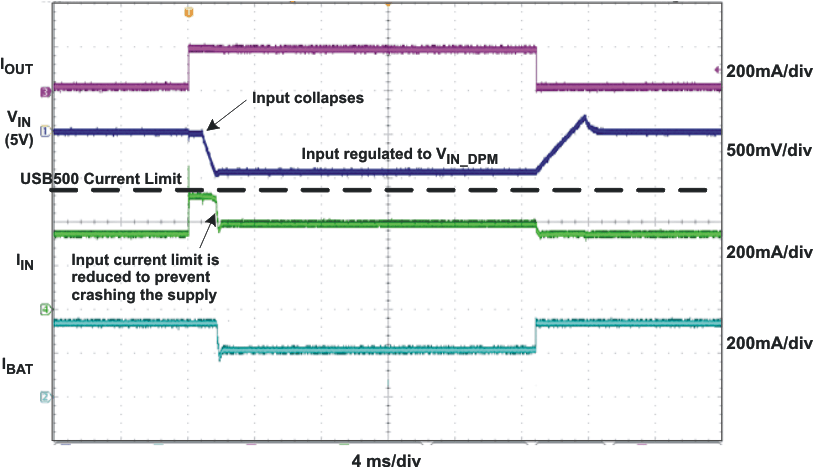 Figure 15. VIN-DPM Waveform
9.3.4.1.2 DPPM Mode
When the sum of the charging and system load currents exceeds the maximum input current (programmed with EN1, EN2, and ILIM pins), the voltage at OUT decreases. Once the voltage on the OUT pin falls to VDPPM, the bq2407x enters DPPM mode. In this mode, the charging current is reduced as the OUT current increases in order to maintain the system output. Battery termination is disabled while in DPPM mode.
9.3.4.1.3 Battery Supplement Mode
While in DPPM mode, if the charging current falls to zero and the system load current increases beyond the programmed input current limit, the voltage at OUT reduces further. When the OUT voltage drops below the VBSUP1 threshold, the battery supplements the system load. The battery stops supplementing the system load when the voltage at OUT rises above the VBSUP2 threshold.
During supplement mode, the battery supplement current is not regulated (BAT-FET is fully on), however there is a short circuit protection circuit built in. Figure 31 demonstrates supplement mode. If during battery supplement mode, the voltage at OUT drops VO(SC2) below the BAT voltage, the OUT output is turned off if the overload exists after tDGL(SC2). The short circuit recovery timer then starts counting. After tREC(SC2), OUT turns on and attempts to restart. If the short circuit remains, OUT is turned off and the counter restarts. Battery termination is disabled while in supplement mode.
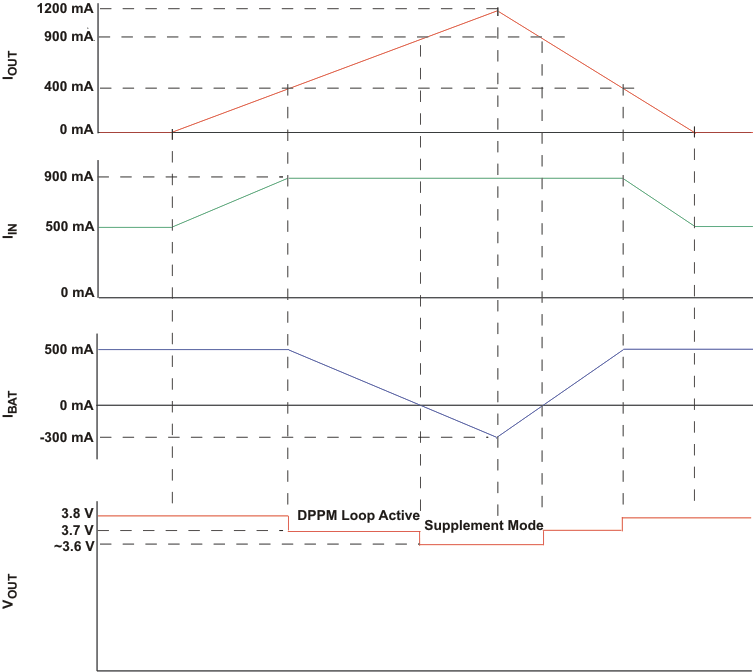 Figure 16. bq24076/78 DPPM and Battery Supplement Modes (VOREG = VBAT + 210 mV, VBAT = 3.6 V)
9.3.4.2 Input Source Not Connected
When no source is connected to the IN input, OUT is powered strictly from the battery. During this mode the current into OUT is not regulated, similar to Battery Supplement Mode, however the short circuit circuitry is active. If the OUT voltage falls below the BAT voltage by 250 mV for longer than tDGL(SC2), OUT is turned off. The short circuit recovery timer then starts counting. After tREC(SC2), OUT turns on and attempts to restart. If the short circuit remains, OUT is turned off and the counter restarts. This ON/OFF cycle continues until the overload condition is removed.
9.3.5 Battery Charging
Set CE low to initiate battery charging. First, the device checks for a short-circuit on the BAT pin by sourcing IBAT(SC) to the battery and monitoring the voltage. When the BAT voltage exceeds VBAT(SC), the battery charging continues. The battery is charged in three phases: conditioning pre-charge, constant current fast charge (current regulation) and a constant voltage tapering (voltage regulation). In all charge phases, an internal control loop monitors the IC junction temperature and reduces the charge current if an internal temperature threshold is exceeded.
Figure 17 illustrates a normal Li-Ion charge cycle using the bq2407x:
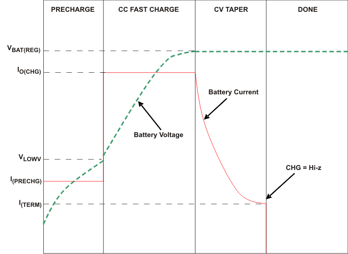 Figure 17. Typical Charge Cycle
In the pre-charge phase, the battery is charged at with the pre-charge current (IPRECHG). Once the battery voltage crosses the VLOWV threshold, the battery is charged with the fast-charge current (ICHG). As the battery voltage reaches VBAT(REG), the battery is held at a constant voltage of VBAT(REG) and the charge current tapers off as the battery approaches full charge. When the battery current reaches ITERM, the CHG pin indicates charging done by going high-impedance.
Note that termination detection is disabled whenever the charge rate is reduced because of the actions of the thermal loop, the DPPM loop or the VIN(LOW) loop.
The value of the fast-charge current is set by the resistor connected from the ISET pin to VSS, and is given by the equation:
The charge current limit is adjustable up to 1.5 A. The valid resistor range is 590 Ω to 5.9 kΩ. If ICHG is programmed as greater than the input current limit, the battery will not charge at the rate of ICHG, but at the slower rate of IIN(MAX) (minus the load current on the OUT pin, if any). In this case, the charger timers will be proportionately slowed down.
9.3.5.1 Charge Current Translator
When the charger is enabled, internal circuits generate a current proportional to the charge current at the ISET input. The current out of ISET is 1/400 (±10%) of the charge current. This current, when applied to the external charge current programming resistor, RISET, generates an analog voltage that can be monitored by an external host to calculate the current sourced from BAT.
 Figure 18. Battery Charging Flow Diagram
9.3.5.2 Battery Detection and Recharge
The bq2407x automatically detects if a battery is connected or removed. Once a charge cycle is complete, the battery voltage is monitored. When the battery voltage falls below VRCH, the battery detection routine is run. During battery detection, current (IBAT(DET)) is pulled from the battery for a duration tDET to see if the voltage on BAT falls below VLOWV. If not, charging begins. If it does, then it indicates that the battery is missing or the protector is open. Next, the precharge current is applied for tDET to close the protector if possible. If VBAT < VRCH, then the protector closed and charging is initiated. If VBAT > VRCH, then the battery is determined to be missing and the detection routine continues.
9.3.5.3 Battery Disconnect (SYSOFF Input, bq24076, bq24078)
The bq24076 and bq24078 feature a SYSOFF input that allows the user to turn the FET Q2 off and disconnect the battery from the OUT pin. This is useful for disconnecting the system load from the battery, factory programming where the battery is not installed or for host side impedance track fuel gauging, such as bq27500, where the battery open circuit voltage level must be detected before the battery charges or discharges. The /CHG output remains low when SYSOFF is high. Connect SYSOFF to VSS, to turn Q2 on for normal operation. SYSOFF is internally pulled to VBAT through ~5 MΩ resistor.
9.3.5.4 Dynamic Charge Timers (TMR Input)
The bq2407x devices contain internal safety timers for the pre-charge and fast-charge phases to prevent potential damage to the battery and the system. The timers begin at the start of the respective charge cycles. The timer values are programmed by connecting a resistor from TMR to VSS. The resistor value is calculated using the following equation:
Leave TMR unconnected to select the internal default timers. Disable the timers by connecting TMR to VSS.
Reset the timers by toggling the CE pin, or by toggling EN1, EN2 pin to put the device in and out of USB suspend mode (EN1 = HI, EN2 = HI).
Note that timers are suspended when the device is in thermal shutdown, and the timers are slowed proportionally to the charge current when the device enters thermal regulation.
During the fast charge phase, several events increase the timer durations.
- The system load current activates the DPPM loop which reduces the available charging current
- The input current is reduced because the input voltage has fallen to VIN(LOW)
- The device has entered thermal regulation because the IC junction temperature has exceeded TJ(REG)
During each of these events, the internal timers are slowed down proportionately to the reduction in charging current. For example, if the charging current is reduced by half for two minutes, the timer clock is reduced to half the frequency and the counter counts half as fast resulting in only one minute of "counting" time.
If the pre charge timer expires before the battery voltage reaches VLOWV, the bq2407x indicates a fault condition. Additionally, if the battery current does not fall to ITERM before the fast charge timer expires, a fault is indicated. The CHG output flashes at approximately 2 Hz to indicate a fault condition. The fault condition is cleared by toggling CE or the input power, entering/ exiting USB suspend mode, or an OVP event.
9.3.5.5 Status Indicators (PGOOD, CHG)
The bq2407x contains two open-drain outputs that signal its status. The PGOOD output signals when a valid input source is connected. PGOOD is low when (VBAT + VIN(DT)) < VIN < VOVP. When the input voltage is outside of this range, PGOOD is high impedance.
The charge cycle after power-up, CE going low, or exiting OVP is indicated with the CHG pin on (low - LED on), whereas all refresh (subsequent) charges will result in the CHG pin off (open - LED off). In addition, the CHG signals timer faults by flashing at approximately 2 Hz.
Table 1. PGOOD Status Indicator
| INPUT STATE | PGOOD OUTPUT |
|---|---|
| VIN < VUVLO | High-impedance |
| VUVLO < VIN < VBAT + VIN(DT) | High-impedance |
| VBAT + VIN(DT) < VIN < VOVP | Low |
| VIN > VOVP | High-impedance |
Table 2. CHG Status Indicator
| CHARGE STATE | CHG OUTPUT |
|---|---|
| Charging | Low (for first charge cycle) |
| Charging suspended by thermal loop | |
| Safety timers expired | Flashing at 2 Hz |
| Charging done | High-impedance |
| Recharging after termination | |
| IC disabled or no valid input power | |
| Battery absent |
9.3.5.6 Thermal Regulation and Thermal Shutdown
The bq2407x contain a thermal regulation loop that monitors the die temperature. If the temperature exceeds TJ(REG), the device automatically reduces the charging current to prevent the die temperature from increasing further. In some cases, the die temperature continues to rise despite the operation of the thermal loop, particularly under high VIN and heavy OUT system load conditions. Under these conditions, if the die temperature increases to TJ(OFF), the input FET Q1 is turned OFF. FET Q2 is turned ON to ensure that the battery still powers the load on OUT. Once the device die temperature cools by TJ(OFF-HYS), the input FET Q1 is turned on and the device returns to thermal regulation. Continuous overtemperature conditions result in a "hiccup" mode. During thermal regulation, the safety timers are slowed down proportionately to the reduction in current limit.
Note that this feature monitors the die temperature of the bq2407x. This is not synonymous with ambient temperature. Self heating exists due to the power dissipated in the IC because of the linear nature of the battery charging algorithm and the LDO associated with OUT. A modified charge cycle with the thermal loop active is shown in Figure 19. Battery termination is disabled during thermal regulation.
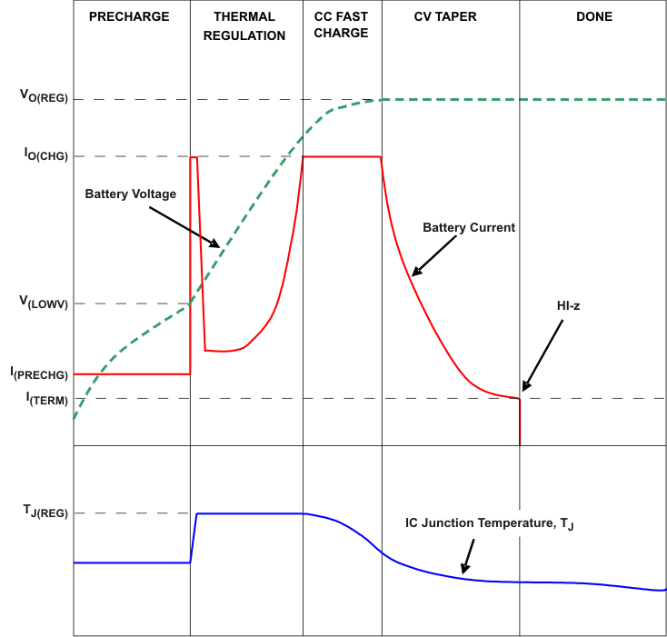 Figure 19. Charge Cycle Modified by Thermal Loop
9.3.6 Battery Pack Temperature Monitoring
The bq2407x features an external battery pack temperature monitoring input. The TS input connects to the NTC thermistor in the battery pack to monitor battery temperature and prevent dangerous over-temperature conditions. During charging, INTC is sourced to TS and the voltage at TS is continuously monitored. If, at any time, the voltage at TS is outside of the operating range (VCOLD to VHOT), charging is suspended. The timers maintain their values but suspend counting. When the voltage measured at TS returns to within the operation window, charging is resumed and the timers continue counting. When charging is suspended due to a battery pack temperature fault, the CHG pin remains low and continues to indicate charging.
For applications that do not require the TS monitoring function, connect a 10-kΩ resistor from TS to VSS to set the TS voltage at a valid level and maintain charging.
The allowed temperature range for 103AT-2 type thermistor is 0°C to 50°C. However, the user may increase the range by adding two external resistors. See Figure 20 for the circuit details. The values for Rs and Rp are calculated using the following equations:


where
- RTH: Thermistor Hot Trip Value found in thermistor data sheet
- RTC: Thermistor Cold Trip Value found in thermistor data sheet
- VH: IC's Hot Trip Threshold = 0.3 V nominal
- VC: IC's Cold Trip Threshold = 2.1 V nominal
- ITS: IC's Output Current Bias = 75 µA nominal
- NTC Thermsitor Semitec 103AT-4
Rs and Rp 1% values were chosen closest to calculated values in Table 3.
Table 3. Calculated Values
| COLD TEMP RESISTANCE AND TRIP THRESHOLD, Ω (°C) | HOT TEMP RESISTANCE AND TRIP THRESHOLD, Ω (°C) | EXTERNAL BIAS RESISTOR, Rs (Ω) | EXTERNAL BIAS RESISTOR, Rp (Ω) |
|---|---|---|---|
| 28000 (–0.6) | 4000 (51) | 0 | ∞ |
| 28480 (–1) | 3536 (55) | 487 | 845000 |
| 28480 (–1) | 3021 (60) | 1000 | 549000 |
| 33890 (–5) | 4026 (51) | 76.8 | 158000 |
| 33890 (–5) | 3536 (55) | 576 | 150000 |
| 33890 (–5) | 3021 (60) | 1100 | 140000 |
RHOT and RCOLD are the thermistor resistance at the desired hot and cold temperatures, respectively. The temperature window cannot be tightened more than using only the thermistor connected to TS, it can only be extended.
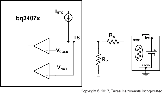 Figure 20. Extended TS Pin Thresholds
9.4 Device Functional Modes
9.4.1 Sleep Mode
When the input is between UVLO and VIN(DT), the device enters sleep mode. After entering sleep mode for >20 mS the internal FET connection between the IN and OUT pin is disabled and pulling the input to ground will not discharge the battery, other than the leakage on the BAT pin. If one has a full 1000-mAHr battery and the leakage is 10 μA, then it would take 1000 mAHr / 10 μA = 100000 hours (11.4 years) to discharge the battery. The self-discharge of the battery is typically five times higher than this.
9.4.2 Explanation of Deglitch Times and Comparator Hysteresis
NOTE
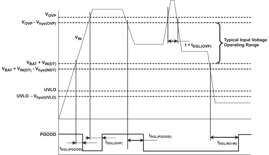 Figure 21. Power-Up, Power-Down, Power Good Indication
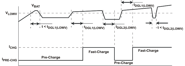 Figure 22. Precharge to Fast-Charge, Fast- to Pre-Charge Transition – tDGL1(LOWV), tDGL2(LOWV)
 Figure 23. Recharge – tDGL(RCH)
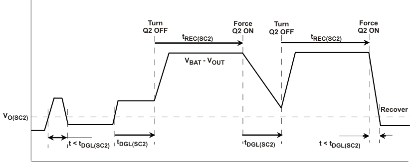 Figure 24. OUT Short-Circuit – Supplement Mode
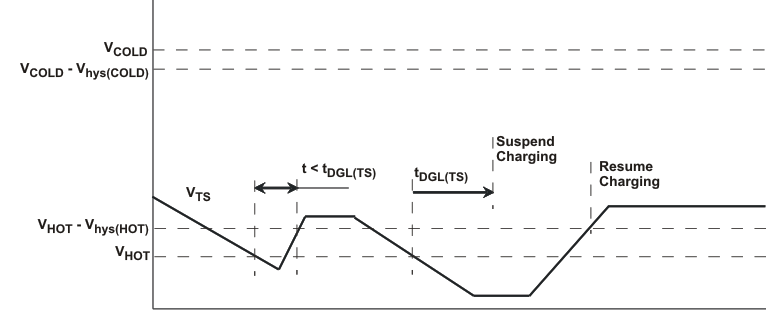 Figure 25. Battery Pack Temperature Sensing – TS Pin. Battery Temperature Increasing