SLUSCM1A October 2017 – December 2017
PRODUCTION DATA.
- 1 Features
- 2 Applications
- 3 Description
- 4 Revision History
- 5 Description (continued)
- 6 Device Comparison Table
- 7 Pin Configuration and Functions
- 8 Specifications
- 9 Detailed Description
- 10Application and Implementation
- 11Power Supply Recommendations
- 12Layout
- 13Device and Documentation Support
- 14Mechanical, Packaging, and Orderable Information
Package Options
Mechanical Data (Package|Pins)
- RGT|16
Thermal pad, mechanical data (Package|Pins)
- RGT|16
Orderable Information
10 Application and Implementation
NOTE
Information in the following applications sections is not part of the TI component specification, and TI does not warrant its accuracy or completeness. TI’s customers are responsible for determining suitability of components for their purposes. Customers should validate and test their design implementation to confirm system functionality.
10.1 Application Information
The bq2407x devices power the system while simultaneously and independently charging the battery. The input power source for charging the battery and running the system can be an AC adapter or a USB port. The devices feature dynamic power-path management (DPPM), which shares the source current between the system and battery charging and automatically reduces the charging current if the system load increases. When charging from a USB port, the input dynamic power management (VIN-DPM) circuit reduces the input current limit if the input voltage falls below a threshold, preventing the USB port from crashing. The power-path architecture also permits the battery to supplement the system current requirements when the adapter cannot deliver the peak system currents.
The bq2407x is configurable to be host controlled for selecting different input current limits based on the input source connected, or a fully stand alone device for applications that do not support multiple types of input sources.
10.2 Typical Application
VIN = UVLO to VOVP, IFASTCHG = 800 mA, IIN(MAX) = 1.3 A, Battery Temperature Charge Range = 0°C to 50°C, 6.25-hour Fastcharge Safety Timer
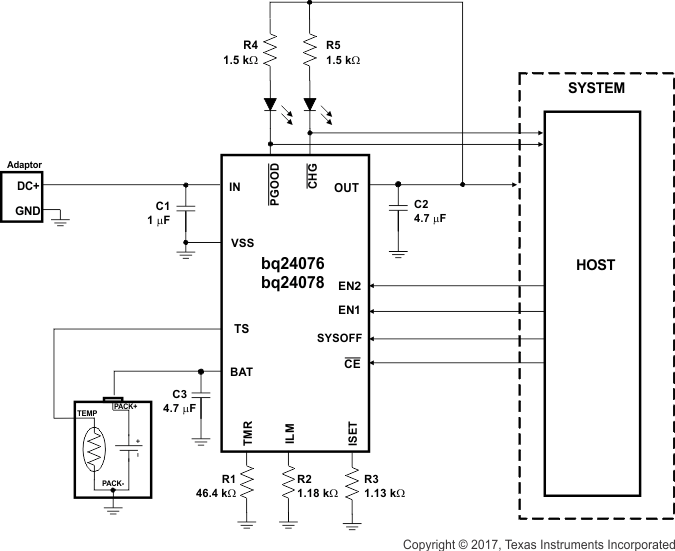 Figure 26. Using bq24076/bq24078 in a Host-Controlled Charger Application
10.2.1 Design Requirements
- Supply voltage = 5 V
- Fast charge current of approximately 800 mA; ISET - pin 16
- Input current limit = 1.3 A; ILIM - pin 12
- Termination current threshold = 110 mA; ITERM – pin 15 (bq24074 only)
- Safety timer duration, Fast-Charge = 6.25 hours; TMR – pin 14
- TS – Battery Temperature Sense = 10 kΩ NTC (103AT-2)
10.2.2 Detailed Design Procedure
10.2.2.1 bq2407x Charger Design Example
See Figure 26 for a schematic of the design example.
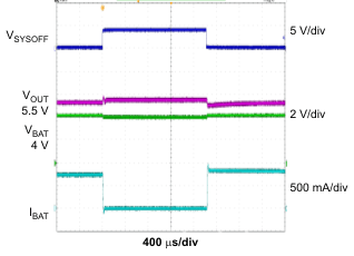
10.2.2.1.1 System ON/OFF (SYSOFF) (bq24076 or bq24078 only)
Connect SYSOFF high to disconnect the battery from the system load. Connect SYSOFF low for normal operation
10.2.2.2 Calculations
10.2.2.2.1 Program the Fast Charge Current (ISET):
RISET = KISET / ICHG
KISET = 890 AΩ from the electrical characteristics table.
RISET = 890 AΩ / 0.8 A = 1.1125 kΩ
Select the closest standard value, which for this case is 1.13 kΩ. Connect this resistor between ISET (pin 16) and VSS.
10.2.2.2.2 Program the Input Current Limit (ILIM)
RILIM = KILIM / II_MAX
KILIM = 1550 AΩ from the electrical characteristics table.
RISET = 1550 AΩ / 1.3 A = 1.192 kΩ
Select the closest standard value, which for this case is 1.18 kΩ. Connect this resistor between ILIM (pin 12) and VSS.
10.2.2.2.3 Program 6.25-hour Fast-Charge Safety Timer (TMR)
RTMR = tMAXCHG / (10 × KTMR )
KTMR = 48 s/kΩ from the electrical characteristics table.
RTMR = (6.25 hr × 3600 s/hr) / (10 × 48 s/kΩ) = 46.8 kΩ
Select the closest standard value, which for this case is 46.4 kΩ. Connect this resistor between TMR (pin 2) and VSS.
10.2.2.3 TS Function
Use a 10-kΩ NTC thermistor in the battery pack (103AT-2). For applications that do not require the TS monitoring function, connect a 10-kΩ resistor from TS to VSS to set the TS voltage at a valid level and maintain charging.
10.2.2.4 CHG and PGOOD
LED Status: Connect a 1.5-kΩ resistor in series with a LED between OUT and CHG to indicate charging status. Connect a 1.5-kΩ resistor in series with a LED between OUT and PGOOD to indicate when a valid input source is connected.
Processor Monitoring Status: Connect a pullup resistor (on the order of 100 kΩ) between the power rail of the processor and CHG and PGOOD.
10.2.2.5 Selecting IN, OUT, and BAT Pin Capacitors
In most applications, all that is needed is a high-frequency decoupling capacitor (ceramic) on the power pin, input, output and battery pins. Using the values shown on the application diagram, is recommended. After evaluation of these voltage signals with real system operational conditions, one can determine if capacitance values can be adjusted toward the minimum recommended values (DC load application) or higher values for fast high amplitude pulsed load applications. Note if designed high input voltage sources (bad adaptors or wrong adaptors), the capacitor needs to be rated appropriately. Ceramic capacitors are tested to 2x their rated values so a 16-V capacitor may be adequate for a 30-V transient (verify tested rating with capacitor manufacturer).
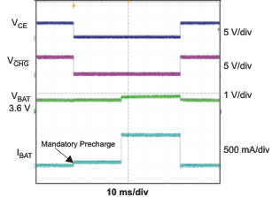
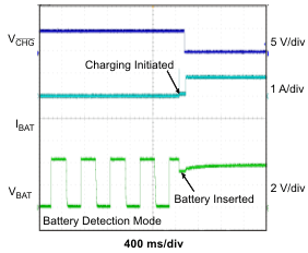
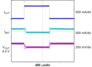
10.2.3 Application Curves
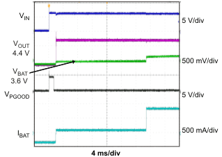
| RLOAD = 10 Ω |
Battery Connected
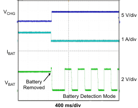
Battery Removed
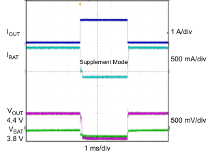
| RLOAD = 25 Ω to 4.5 Ω |
| VIN = 6 V |
bq24076, bq24078
Battery Inserted
| RLOAD = 20 Ω to 9 Ω |
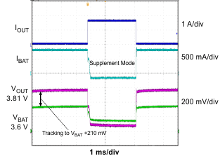
| RLOAD = 20 Ω to 4.5 Ω |
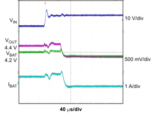
| VIN = 6 V to 15 V | RLOAD = 10 Ω |
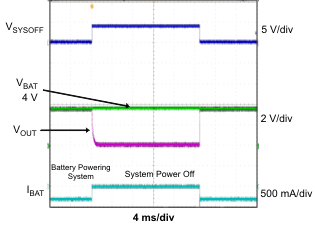
| VIN = 0 V |
bq24076, bq24078