SLUS784E December 2007 – December 2015
PRODUCTION DATA.
- 1 Features
- 2 Applications
- 3 Description
- 4 Revision History
- 5 Device Options
- 6 Pin Configuration and Functions
- 7 Specifications
-
8 Detailed Description
- 8.1 Overview
- 8.2 Functional Block Diagram
- 8.3
Feature Description
- 8.3.1 Control Logic Overview
- 8.3.2 Temperature Qualification (Applies Only to Versions With TS Pin Option)
- 8.3.3 Input Overvoltage Detection, Power Good Status Output
- 8.3.4 Charge Status Outputs
- 8.3.5 Battery Charging: Constant Current Phase
- 8.3.6 Charge Current Translator
- 8.3.7 Battery Voltage Regulation
- 8.3.8 Pre-Charge Timer
- 8.3.9 Thermal Protection Loop
- 8.3.10 Thermal Shutdown And Protection
- 8.3.11 Dynamic Timer Function
- 8.3.12 Charge Termination Detection and Recharge
- 8.3.13 Battery Absent Detection - Voltage Mode Algorithm
- 8.3.14 Charge Safety Timer
- 8.3.15 Short-Circuit Protection
- 8.3.16 Startup With Deeply Depleted Battery Connected
- 8.4 Device Functional Modes
- 9 Application and Implementation
- 10Power Supply Recommendations
- 11Layout
- 12Device and Documentation Support
- 13Mechanical, Packaging, and Orderable Information
Package Options
Refer to the PDF data sheet for device specific package drawings
Mechanical Data (Package|Pins)
- DRC|10
Thermal pad, mechanical data (Package|Pins)
- DRC|10
Orderable Information
7 Specifications
7.1 Absolute Maximum Ratings(1)
| MIN | MAX | UNIT | ||
|---|---|---|---|---|
| Supply voltage (IN with respect to Vss) | –0.3 | 20 | V(2) | |
| Input voltage on IN, STATx, PG, TS, CE, TMR (all with respect to Vss) | –0.3 | V(IN) | V | |
| Input voltage on OUT, BAT, ISET (all with respect to Vss) | –0.3 | 7 | V | |
| Output sink current (STATx) + PG | 15 | mA | ||
| Output current (OUT pin) | 2 | A | ||
| TA | Operating free-air temperature | –40 | 155 | °C |
| TJ | Junction temperature | –40 | 150 | °C |
| Tstg | Storage temperature | –65 | 150 | °C |
(1) Stresses beyond those listed under Absolute Maximum Ratings may cause permanent damage to the device. These are stress ratings only, and functional operation of the device at these or any other conditions beyond those indicated under Recommended Operating Conditions is not implied. Exposure to absolute–maximum–rated conditions for extended periods may affect device reliability.
(2) The bq24085/6/7/8 family can withstand up to 18 V maximum continuously, 20 V for maximum of 2000 hours and 26 V for a maximum for 87 hours.
7.2 ESD Ratings
| VALUE | UNIT | |||
|---|---|---|---|---|
| V(ESD) | Electrostatic discharge | Human-body model (HBM), per ANSI/ESDA/JEDEC JS-001(1) | ±3000 | V |
| Charged-device model (CDM), per JEDEC specification JESD22-C101(2) | ±1500 | |||
(1) JEDEC document JEP155 states that 500-V HBM allows safe manufacturing with a standard ESD control process.
(2) JEDEC document JEP157 states that 250-V CDM allows safe manufacturing with a standard ESD control process.
7.3 Recommended Operating Conditions
| MIN | MAX | UNIT | |||
|---|---|---|---|---|---|
| V(IN) | Supply voltage | Battery absent detection not functional | 3.5 | 4.35 | V |
| V(IN) | Supply voltage | Battery absent detection functional | 4.35 | 6.5 | V |
| R(TMR) | Safety timer program resistor | 33 | 100 | KΩ | |
| TJ | Junction temperature | 0 | 125 | °C | |
7.4 Thermal Information
| THERMAL METRIC(1) | bq2408x | UNIT | |
|---|---|---|---|
| DRC (VSON) | |||
| 10 PINS | |||
| RθJA | Junction-to-ambient thermal resistance | 46.7 | °C/W |
| RθJC(top) | Junction-to-case (top) thermal resistance | 65.9 | °C/W |
| RθJB | Junction-to-board thermal resistance | 21.3 | °C/W |
| ψJT | Junction-to-top characterization parameter | 1.6 | °C/W |
| ψJB | Junction-to-board characterization parameter | 21.4 | °C/W |
| RθJC(bot) | Junction-to-case (bottom) thermal resistance | 3.6 | °C/W |
(1) For more information about traditional and new thermal metrics, see the Semiconductor and IC Package Thermal Metrics application report, SPRA953.
7.5 Electrical Characteristics
over recommended operating range, TJ = 0 –125°C range, See the Application and Implementation section, typical values at TJ = 25°C (unless otherwise noted), RTMR = 49.9 KΩ| PARAMETER | TEST CONDITIONS | MIN | TYP | MAX | UNIT | ||
|---|---|---|---|---|---|---|---|
| POWER DOWN THRESHOLD – UNDERVOLTAGE LOCKOUT | |||||||
| VUVLO | Power down threshold | V(IN) = 0 V, increase V(OUT): 0 → 3 V OR V(OUT) = 0 V, increase V(IN): 0 → 3 V, CE = LO (1) |
1.5 | 3 | V | ||
| INPUT POWER DETECTION(2) | |||||||
| VIN(DT) | Input power detection threshold | V(IN) detected at [V(IN) – V(OUT)] > VIN(DT) | 130 | mV | |||
| VHYS(INDT) | Input power detection hysteresis | Input power not detected at [V(IN) – V(OUT)] < [VIN(DT) – VHYS(INDT)] |
30 | mV | |||
| INPUT OVERVOLTAGE PROTECTION | |||||||
| V(OVP) | Input overvoltage detection threshold | V(IN) increasing | bq24088 | 10.2 | 10.5 | 11.7 | V |
| bq24085/6/7 | 6.2 | 6.5 | 7 | ||||
| VHYS(OVP) | Input overvoltage hysteresis | V(IN) decreasing | bq24088 | 0.5 | V | ||
| bq24085/6/7 | 0.2 | ||||||
| QUIESCENT CURRENT | |||||||
| ICC(CHGOFF) | IN pin quiescent current, charger off | Input power detected, CE = HI |
V(IN) = 6 V | 100 | 200 | μA | |
| V(IN) = 16.5 V | 350 | ||||||
| ICC(CHGON) | IN pin quiescent current, charger on | Input power detected, CE = LO, VBAT = 4.5 V | 4 | 6 | mA | ||
| IBAT(DONE) | Battery leakage current after termination into IC | Input power detected, charge terminated, CE = LO |
1 | 5 | μA | ||
| IBAT(CHGOFF) | Battery leakage current into IC, charger off | Input power detected, CE = HI OR
input power not detected, CE = LO |
1 | 5 | μA | ||
| TS PIN COMPARATOR | |||||||
| V(TS1) | Lower voltage temperature threshold | Hot detected at V(TS) < V(TS1); NTC thermistor | 29 | 30 | 31 | %V(IN) | |
| V(TS2) | Upper voltage temperature threshold | Cold detected at V(TS) > V(TS2); NTC thermistor | 60 | 61 | 62 | %V(IN) | |
| VHYS(TS) | Hysteresis | Temp OK at V(TS) > [ V(TS1) + VHYS(TS) ] OR V(TS) < [ V(TS2) – VHYS(TS) ] |
2 | %V(IN) | |||
| CE INPUT | |||||||
| VIL | Input (low) voltage | V(/CE) | 0 | 1 | V | ||
| VIH | Input (high) voltage | V(/CE) | 2 | V | |||
| STAT1, STAT2 AND PG OUTPUTS(3) | |||||||
| VOL | Output (low) saturation voltage | Iout = 1 mA (sink) | 200 | mV | |||
| THERMAL SHUTDOWN | |||||||
| T(SHUT) | Temperature trip | Junction temperature, temp rising | 155 | °C | |||
| T(SHUTHYS) | Thermal hysteresis | Junction temperature | 20 | °C | |||
| VOLTAGE REGULATION(4) | |||||||
| VO(REG) | Output voltage | 4.20 | V | ||||
| VO(TOL) | Voltage regulation accuracy | TA = 25°C | –0.5% | 0.5% | |||
| –1% | 1% | ||||||
| V(DO) | Dropout voltage, V(IN) – V(OUT) | I(OUT) = 750 mA | 600 | mV | |||
| CURRENT REGULATION(5) | |||||||
| IO(OUT) | Output current range | V(BAT) > V(LOWV), IO(OUT) = I(OUT) = K(SET) × V(SET)/R(SET) | 50 | 750 | mA | ||
| V(SET) | Output current set voltage | V(ISET) = V(SET), V(LOWV) < V(BAT) ≤ VO(REG) | 2.45 | 2.5 | 2.55 | V | |
| K(SET) | Output current set factor | 100 mA ≤ IO(OUT) ≤ 750 mA | 175 | 182 | 190 | ||
| 10 mA ≤ IO(OUT) < 100 mA | 180 | 215 | 250 | ||||
| RISET | External resistor range | Resistor connected to ISET pin | 0.6 | 10 | kΩ | ||
| PRECHARGE AND OUTPUT SHORT-CIRCUIT CURRENT REGULATION(6) | |||||||
| V(LOWV) | Precharge to fast-charge transition threshold | V(BAT) increasing | 2.8 | 2.95 | 3.15 | V | |
| V(SC) | Precharge to short-circuit transition threshold | V(BAT) decreasing | 1.2 | 1.4 | 1.6 | V | |
| V(SCIND) | Short-circuit indication | V(BAT) decreasing | 1.6 | 1.8 | 2 | ||
| IO(PRECHG) | Precharge current range | V(SC) < VI(BAT) < V(LOWV), t < t(PRECHG)
IO(PRECHG) = K(SET) × V(PRECHG)/R(ISET) |
5 | 75 | mA | ||
| V(PRECHG) | Precharge set voltage | V(ISET) = V(PRECHG), V(SC) < VI(BAT) < V(LOWV), t < t(PRECHG) |
225 | 250 | 280 | mV | |
| IO(SHORT) | Output shorted regulation current | VSS ≤ V(BAT) ≤ V(SCI), IO(SHORT) = I(OUT), V(BAT)= VSS, Internal pullup resistor, TJ = 25°C |
VPOR < VIN < 6.0 V | 7 | 15 | 24 | mA |
| 6.0 V < VIN < VOVP | 15 | ||||||
| TEMPERATURE REGULATION (Thermal regulation™)(7) | |||||||
| TJ(REG) | Temperature regulation limit | V(IN) = 5.5 V, V(BAT) = 3.2 V, Fast charge current set to 1 A | 101 | 112 | 125 | °C | |
| I(MIN_TJ(REG)) | Minimum current in thermal regulation | V(LOWV) < V(BAT) < VO(REG), 0.7 kΩ < R(ISET) < 1.18 kΩ |
105 | 125 | mA | ||
| CHARGE TERMINATION DETECTION(9) | |||||||
| I(TERM) | Termination detection current range | V(BAT) > V(RCH), I(TERM) = K(SET) × V(TERM)/R(ISET) | 5 | 75 | mA | ||
| V(TERM) | Charge termination detection set voltage(8) | V(BAT) > V(RCH) | 225 | 250 | 275 | mV | |
| BATTERY RECHARGE THRESHOLD | |||||||
| V(RCH) | Recharge threshold detection | [VO(REG)–V(BAT) ] > V(RCH) | 75 | 100 | 135 | mV | |
| TIMERS(10) | |||||||
| VTMR(OFF) | Charge timer and termination enable threshold | Charge timer AND termination disabled at: V(TMR) > VTMR(OFF) | bq24085/86/88 | 2.5 | 3 | 3.5 | V |
| Charge timer enable threshold | Charge timer disabled at: V(TMR) > VTMR(OFF) |
bq24087 | |||||
| BATTERY DETECTION THRESHOLDS | |||||||
| IDET(DOWN) | Battery detection current (sink) | 2 V < V(BAT) < VO(REG) | 1 | 2 | 3.2 | mA | |
| IDET(UP) | Battery detection current (source) | 2 V < V(BAT) < VO(REG) | IO(PRECHG) | mA | |||
| TIMER FAULT RECOVERY | |||||||
| I(FAULT) | Fault Current (source) | V(OUT) < V(RCH) | 0.8 | 1.1 | mA | ||
| OUTPUT CURRENT SAFETY LIMIT(11) | |||||||
| I(SETSC) | Charge overcurrent safety | V(ISET) = VSS | 1.5 | A | |||
(1) Specified by design, not production tested.
(2) CE = HI or LOW, V(IN) > 3.5 V
(3) V(IN) ≥ VO(REG) + V(DO-MAX)
(4) V(IN) ≥ VO(REG) + V(DO-MAX), I(TERM) < I(OUT) < IO(OUT), charger enabled, no fault conditions detected.
(5) V(IN) > V(OUT) > V(DO-MAX), charger enabled, no fault conditions detected.
(6) V(IN)–V(OUT) > V(DO-MAX) , V(IN) ≥ 4.5 V, charger enabled, no fault conditions detected, RTMR = 50 K or V(TMR)=OPEN; thermal regulation loop not active.
(7) Charger enabled, no fault conditions detected.
(8) The voltage on the ISET pin is compared to the V(TERM) voltage to determine when the termination should occur.
(9) VO(REG) = 4.2 V, charger enabled, no fault conditions detected, thermal regulation loop not active, RTMR = 50 K or TMR pin open.
(10) CE = LO, charger enabled, no fault conditions detected, V(TMR) < 3 V, timers enabled.
(11) V(IN) ≥ 4.5 V, charger enabled, ISET shorted to GND.
7.6 Timing Requirements
over recommended operating range, TJ = 0 –125°C range, See the Application and Implementation section, typical values at TJ = 25°C (unless otherwise noted), RTMR = 49.9 KΩ| PARAMETER | TEST CONDITIONS | MIN | TYP | MAX | UNIT | ||
|---|---|---|---|---|---|---|---|
| POWER DOWN THRESHOLD – UNDERVOLTAGE LOCKOUT | |||||||
| tDGL(PG) | Deglitch time on power good | V(IN) = 0 V → 5 V in 1 μs to PG:HI → LO |
2 | ms | |||
| INPUT POWER DETECTION(1) | |||||||
| tDGL(NOIN) | Delay time, input power not detected status(2) | PG: LO →HI after tDGL(NOIN) | 10 | μs | |||
| tDLY(CHGOFF) | Charger off delay | Charger turned off after tDLY(CHGOFF), Measured from PG: LO → HI; Timer reset after tDLY(CHGOFF) | 25 | ms | |||
| INPUT OVERVOLTAGE PROTECTION | |||||||
| tDGL(OVDET) | Input overvoltage detection delay | CE = HI or LO, Measured from V(IN) > V(OVP) to PG: LO → HI; VIN increasing |
100 | μs | |||
| tDGL(OVNDET) | Input overvoltage not detected delay(2) | CE = HI or LO, Measured from V(IN) < V(OVP)
to PG: HI → LO; V(IN) decreasing |
100 | μs | |||
| VOLTAGE AND CURRENT REGULATION TIMING(3) | |||||||
| tPWRUP(CHG) | Input power detection to full charge current time delay | Measured from PG:HI → LO to I(OUT) > 100 mA, CE = LO, IO(OUT) = 750 mA, V(BAT) = 3.5 V |
25 | ms | |||
| tPWRUP(EN) | Charge enable to full charge current delay | Measured from CE:HI → LO to I(OUT) >100 mA, IO(OUT) = 750 mA, V(BAT)= 3.5 V, V(IN) = 4.5 V, Input power detected | 25 | ms | |||
| tPWRUP(LDO) | Input power detection to voltage regulation delay, LDO mode set, no battery or load connected | Measured from PG:HI → LO to V(OUT) > 90% of charge voltage regulation; V(TMR) = OPEN, LDO mode set, no battery and no load at OUT pin, CE = LO |
25 | ms | |||
| CHARGE TERMINATION DETECTION(4) | |||||||
| tDGL(TERM) | Deglitch time, termination detected | V(ISET) decreasing | 50 | ms | |||
| BATTERY RECHARGE THRESHOLD | |||||||
| tDGL(RCH) | Deglitch time, recharge detection | V(BAT) decreasing | 350 | ms | |||
| TIMERS(5) | |||||||
| t(CHG) | Charge safety timer range | t(CHG) = K(CHG) × RTMR ; thermal loop not active | 3 | 10 | hours | ||
| K(CHG) | Charge safety timer constant | V(BAT) > V(LOWV) | 0.08 | 0.1 | 0.12 | hr/kΩ | |
| t(PCHG) | Pre-charge safety timer range | t(PCHG) = K(PCHG) × t(CHG) ; Thermal regulation loop not active | 1080 | 3600 | s | ||
| K(PCHG) | Pre-charge safety timer constant | V(BAT) < V(LOWV) | 0.08 | 0.1 | 0.12 | ||
| BATTERY DETECTION THRESHOLDS | |||||||
| t(DETECT) | Battery detection time | 2 V < V(BAT) < VO(REG), Thermal regulation loop not active; RTMR = 50 kΩ, IDET(down) or IDET (UP) | 125 | ms | |||
(1) CE = HI or LOW, V(IN) > 3.5 V
(2) Specified by design, not production tested.
(3) V(IN) > V(OUT) + V(DO-MAX), charger enabled, no fault conditions detected, RTMR = 50 K or V(TMR) = OPEN; thermal regulation loop not active.
(4) VO(REG) = 4.2 V, charger enabled, no fault conditions detected, thermal regulation loop not active, RTMR = 50 K or TMR pin open.
(5) CE = LO, charger enabled, no fault conditions detected, V(TMR) < 3 V, timers enabled.
7.7 Dissipation Ratings(1)
| PACKAGE | θJC (°C/W) | θJA (°C/W) |
|---|---|---|
| 10-pin DRC | 3.21 | 46.87 |
(1) This data is based on using the JEDEC High-K board and the exposed die pad is connected to a copper pad on the board. This is connected to the ground plane by a 2×3 via matrix.
7.8 Typical Characteristics
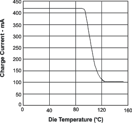
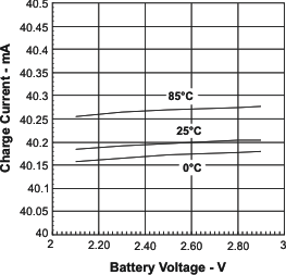
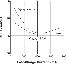
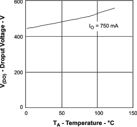
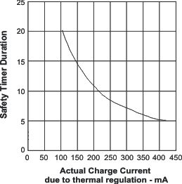
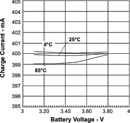
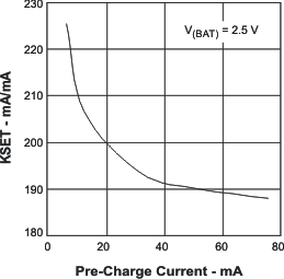
Measured using the typical application circuit shown previously.