SLUSCQ6 October 2016
PRODUCTION DATA.
- 1 Features
- 2 Applications
- 3 Description
- 4 Revision History
- 5 Pin Configuration and Functions
- 6 Specifications
- 7 Typical Characteristics
-
8 Detailed Description
- 8.1 Overview
- 8.2 Functional Block Diagram
- 8.3
Feature Description
- 8.3.1 Device Power Up
- 8.3.2 Battery Switch (Q1 + Q2)
- 8.3.3 Integrated 10-bit ADC for Monitoring
- 8.3.4 Linear Regulation Mode (LDO)
- 8.3.5
Protection Features
- 8.3.5.1 Reverse Current Protection (RCP)
- 8.3.5.2 Internal Thermal Shutdown
- 8.3.5.3 Input Overvoltage Protection
- 8.3.5.4 IBUS and VBUS Protection
- 8.3.5.5 IBAT and VBAT Protection
- 8.3.5.6 VOUT Protection
- 8.3.5.7 VDROP Protection
- 8.3.5.8 VBUS Temperature (TS_BUS_FLT) and Battery Temperature (TS_BAT_FLT)
- 8.3.6 I2C Serial Interface
- 8.4 Device Functional Modes
- 8.5
I2C Register Maps
- 8.5.1 I2C Register Summary Table
- 8.5.2 REG00 (DEVICE_INFO)
- 8.5.3 REG01 (EVENT_1_MASK)
- 8.5.4 REG02 (EVENT_2_MASK)
- 8.5.5 REG03 (EVENT_1)
- 8.5.6 REG04 (EVENT_2)
- 8.5.7 REG05 (EVENT_1_EN)
- 8.5.8 REG06 (CONTROL)
- 8.5.9 REG07 (ADC_CONTROL)
- 8.5.10 REG08 (ADC_EN)
- 8.5.11 REG09 (PROTECTION)
- 8.5.12 REG0A (VBUS_OVP)
- 8.5.13 REG0B (VOUT_REG)
- 8.5.14 REG0C (VDROP_OVP)
- 8.5.15 REG0D (VDROP_ALM)
- 8.5.16 REG0E (VBAT_REG)
- 8.5.17 REG0F (IBAT_REG)
- 8.5.18 REG10 (IBUS_REG)
- 8.5.19 REG11 (TS_BUS_FLT)
- 8.5.20 REG12 (TS_BAT_FLT)
- 8.5.21 REG 13 and REG 14 (VBUS_ADC)
- 8.5.22 REG15 and REG16 (IBUS_ADC)
- 8.5.23 REG17 and REG18 (VOUT_ADC)
- 8.5.24 REG19 and REG1A (VDROP_ADC)
- 8.5.25 REG1B and REG1C (VBAT_ADC)
- 8.5.26 REG1D and REG1E (IBAT_ADC)
- 8.5.27 REG1F and REG20 (TS_BUS_ADC)
- 8.5.28 REG21 and REG22 (TS_BAT_ADC)
- 8.5.29 REG 23 (TDIE_ADC)
- 8.5.30 REG 24 (EVENT_2_EN)
- 8.5.31 REG 25 (EVENT_3_MASK)
- 8.5.32 REG 26 (EVENT_3)
- 8.5.33 REG27 and REG28 (VUSB_ADC)
- 8.5.34 REG 29 (CONTROL_2)
- 8.5.35 REG 40 (DIE_TEMP_FLT)
- 9 Application and Implementation
- 10Power Supply Recommendations
- 11Layout
- 12Device and Documentation Support
- 13Mechanical, Packaging, and Orderable Information
Package Options
Refer to the PDF data sheet for device specific package drawings
Mechanical Data (Package|Pins)
- YFF|42
Thermal pad, mechanical data (Package|Pins)
Orderable Information
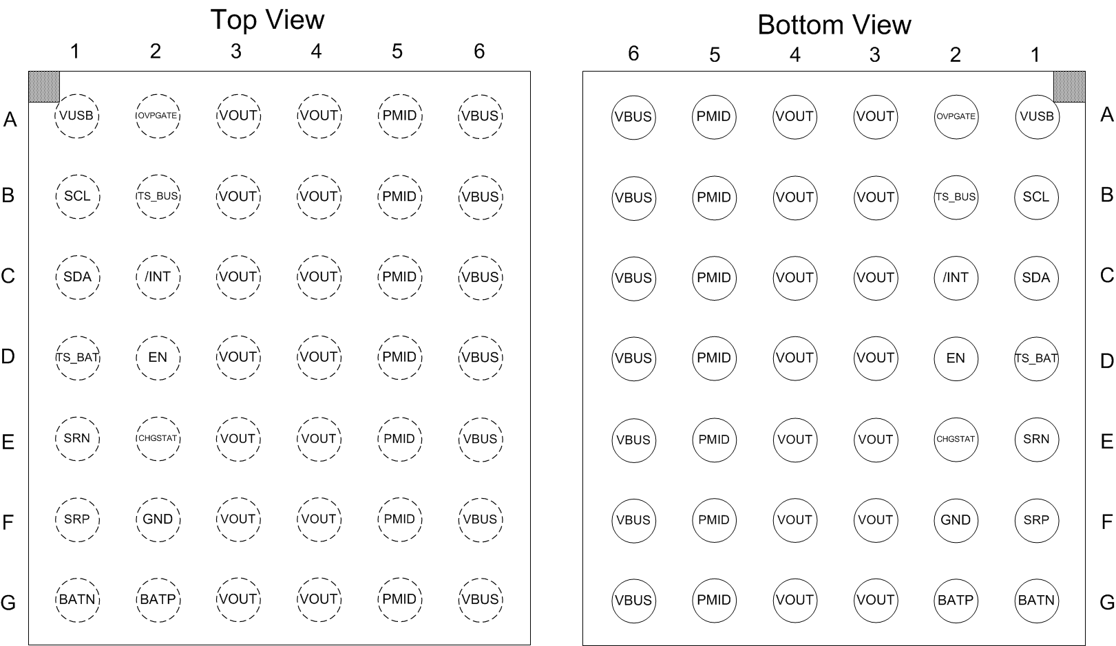
5 Pin Configuration and Functions
DSBGA Package
42 Pin YYF
Top View

Pin Functions
| PIN | I/O | DESCRIPTION | |
|---|---|---|---|
| NAME | NO. | ||
| VOUT | A3-G3, A4-G4 | P | Device power output. Connected to the drain of Q2. |
| PMID | A5-G5 | P | Tie pins to each other and leave floating. Do not connect to any other pins. Connected to the drain of Q1 and source of Q2. |
| TS_BUS | B2 | AI | VBUS connector temperature qualification voltage input. Requires external resistor divider and voltage reference. |
| GND | F2 | P | Device ground. |
| TS_BAT | D1 | AI | Battery temperature qualification voltage input. Requires external resistor divider and voltage reference. |
| BATN | G1 | AI | Negative input for battery voltage sensing. Connect to negative terminal of battery pack. Place 100-Ω/1-kΩ series resistance between pin and negative terminal. |
| BATP | G2 | AI | Positive input for battery voltage sensing. Connect to positive terminal of battery pack. Place 100-Ω/1-kΩ series resistance between pin and positive terminal. |
| SRN | E1 | AI | Negative input for battery current sensing. Place RSENSE between SRN and SRP for battery current sensing. |
| SRP | F1 | AI | Positive input for battery current sensing. Place RSENSE between SRN and SRP for battery current sensing. |
| VBUS | A6, B6, C6, D6, E6, F6, G6 | P | Device power input. |
| EN | D2 | DI | Active high device enable. Pull low to disable device. ADC not available when device is disabled. |
| CHGSTAT | E2 | DI | Open drain, active low battery switch indicator. Connect to pull-up voltage via 10-kΩ pull-up resistor. This pin will assert low if battery switch is enabled and will go high when battery switch is disabled (due to fault or charge disabled or POR event). |
| INT | C2 | DO | Open drain, active low interrupt output. Connect to pull-up voltage via 10-kΩ pull-up resistor. Normally low, the INT pin asserts low to report status and faults. Keep constant low until the host reads this register 0x03, 0x04. |
| SDA | C1 | DIO | I2C interface data. Connect to pull-up voltage via 1-kΩ pull-up resistor. |
| SCL | B1 | DI | I2C interface clock. Connect to pull-up voltage via 1-kΩ pull-up resistor. |
| OVPGATE | A2 | AO | External OVP FET N-channel gate drive pin. |
| VUSB | A1 | AI | Device power input. Place a 500-Ω series resistor between this pin and USB supply voltage. |