SLUSCH6B March 2016 – March 2017
PRODUCTION DATA.
- 1 Features
- 2 Applications
- 3 Description
- 4 Revision History
- 5 Description (Continued)
- 6 Pin Configuration and Functions
- 7 Specifications
-
8 Detailed Description
- 8.1 Functional Block Diagram
- 8.2
Feature Description
- 8.2.1 Device Power-On-Reset (POR)
- 8.2.2 Device Power Up from Battery without Input Source
- 8.2.3 Device Power Up from Input Source
- 8.2.4 Power Path Management
- 8.2.5 Battery Charging Management
- 8.2.6 Battery Monitor
- 8.2.7 Status Outputs (PG, STAT, and INT)
- 8.2.8 Thermal Regulation and Thermal Shutdown
- 8.2.9 Voltage and Current Monitoring in Buck
- 8.2.10 Battery Protection
- 8.2.11 Serial Interface
- 8.3 Device Functional Modes
- 8.4 Register Map
- 9 Application and Implementation
- 10Power Supply Recommendations
- 11Layout
- 12Device and Documentation Support
- 13Mechanical, Packaging, and Orderable Information
Package Options
Mechanical Data (Package|Pins)
- YFF|42
Thermal pad, mechanical data (Package|Pins)
Orderable Information
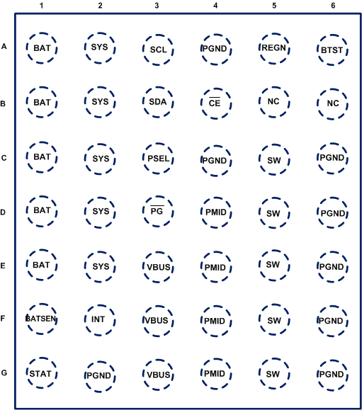
6 Pin Configuration and Functions
YFF Package
42-Pin DSBGA
Top View

Pin Functions
| PIN | TYPE(1) | DESCRIPTION | |
|---|---|---|---|
| NAME | NO. | ||
| VBUS | E3-G3 | P | Charger Input Voltage. The internal n-channel reverse block MOSFET (RBFET) is connected between VBUS and PMID with VBUS on source. Place a 1-uF ceramic capacitor from VBUS to PGND and place it as close as possible to IC. |
| PSEL | C3 | DI | Power source selection input. High indicates a USB host source and Low indicates an adapter source. |
| PG | D3 | DO | Open drain active low power good indicator. Connect to the pull up rail via 10-kohm resistor. LOW indicates a good input source if the input voltage is within VVBUS_OP, above SLEEP mode threshold (VSLEEPZ), and current limit is above IBATSRC (30mA). |
| STAT | G1 | DO | Open-drain interrupt output. Connect to the INT to a logic rail via 10-kohm resistor. The INT pin sends active low, 256-us pulse to host to report charger device status and fault. |
| SCL | A3 | DI | I2C Interface clock. Connect SCL to the logic rail through a 10-kΩ resistor. |
| SDA | B3 | DIO | I2C Interface data. Connect SDA to the logic rail through a 10-kΩ resistor. |
| INT | F2 | DO | Open-drain Interrupt Output. Connect the INT to a logic rail via 10-kΩ resistor. The INT pin sends active low, 256-μs pulse to host to report charger device status and fault. |
| CE | B4 | DI | Active low charge enable pin. Battery charging is enabled when CHG_CONFIG = 1 and CE pin = Low. CE pin must be pulled High or Low. |
| NC | B5-B6 | No connect. Float the pin. | |
| BAT | A1-E1 | P | Battery connection point to the positive terminal of the battery pack. The internal current sensing circuitry is connected between SYS and BAT. Connect a 10uF closely to the BAT pin. |
| SYS | A2-E2 | P | Converter output connection point. The internal current sensing circuitry is connected between SYS and BAT. Connect a 20uF closely to the SYS pin. |
| PGND | C4,C6-G6,A4,G2 | P | Power ground connection for high-current power converter node. Internally, PGND is connected to the source of the n-channel LSFET. On PCB layout, connect directly to ground connection of input and output capacitors of the charger. A single point connection is recommended between power PGND and the analog GND near the IC PGND pin. |
| SW | C5-G5 | P | Switching node connecting to output inductor. Internally SW is connected to the source of the n-channel HSFET and the drain of the n-channel LSFET. Connect the 0.047μF bootstrap capacitor from SW to BTST. |
| BTST | A6 | P | PWM high side driver positive supply. Internally, the BTST is connected to the cathode of the boost-strap diode. Connect the 0.047μF bootstrap capacitor from SW to BTST. |
| REGN | A5 | P | PWM low side driver positive supply output. Internally, REGN is connected to the anode of the boost-strap diode. Connect a 4.7μF (10 V rating) ceramic capacitor from REGN to analog GND. The capacitor should be placed close to the IC. |
| PMID | D4-G4 | DO | Connected to the drain of the reverse blocking MOSFET (RBFET) and the drain of HSFET. Given the total input capacitance, put 1μF on VBUS to PGND, and the rest capacitance on PMID to PGND. |
| BATSEN | F1 | AI | Remote battery sense input. The typical pin resistance is 800 kΩ. Connect as close to battery as possible. |
(1) DI (Digital Input), DO (Digital Output), DIO (Digital Input/Output), AI (Analog Input), AO (Analog Output), AIO (Analog Input/Output)