SLUSCS4C June 2017 – April 2021 BQ40Z50-R2
PRODUCTION DATA
- 1 Features
- 2 Applications
- 3 Description
- 4 Revision History
- 5 Description (continued)
- 6 Pin Configuration and Functions
-
7 Specifications
- 7.1 Absolute Maximum Ratings
- 7.2 ESD Ratings
- 7.3 Recommended Operating Conditions
- 7.4 Thermal Information
- 7.5 Supply Current
- 7.6 Power Supply Control
- 7.7 AFE Power-On Reset
- 7.8 AFE Watchdog Reset and Wake Timer
- 7.9 Current Wake Comparator
- 7.10 VC1, VC2, VC3, VC4, BAT, PACK
- 7.11 SMBD, SMBC
- 7.12 PRES, BTP_INT, DISP
- 7.13 LEDCNTLA, LEDCNTLB, LEDCNTLC
- 7.14 Coulomb Counter
- 7.15 CC Digital Filter
- 7.16 ADC
- 7.17 ADC Digital Filter
- 7.18 CHG, DSG FET Drive
- 7.19 PCHG FET Drive
- 7.20 FUSE Drive
- 7.21 Internal Temperature Sensor
- 7.22 TS1, TS2, TS3, TS4
- 7.23 PTC, PTCEN
- 7.24 Internal 1.8-V LDO
- 7.25 High-Frequency Oscillator
- 7.26 Low-Frequency Oscillator
- 7.27 Voltage Reference 1
- 7.28 Voltage Reference 2
- 7.29 Instruction Flash
- 7.30 Data Flash
- 7.31 OLD, SCC, SCD1, SCD2 Current Protection Thresholds
- 7.32 Timing Requirements: OLD, SCC, SCD1, SCD2 Current Protection Timing
- 7.33 Timing Requirements: SMBus
- 7.34 Timing Requirements: SMBus XL
- 7.35 Typical Characteristics
-
8 Detailed Description
- 8.1 Overview
- 8.2 Functional Block Diagram
- 8.3
Feature Description
- 8.3.1 Primary (1st Level) Safety Features
- 8.3.2 Secondary (2nd Level) Safety Features
- 8.3.3 Charge Control Features
- 8.3.4 Gas Gauging
- 8.3.5 Configuration
- 8.3.6 Battery Parameter Measurements
- 8.3.7 Battery Trip Point (BTP)
- 8.3.8 Lifetime Data Logging Features
- 8.3.9 Authentication
- 8.3.10 LED Display
- 8.3.11 IATA Support
- 8.3.12 Voltage
- 8.3.13 Current
- 8.3.14 Temperature
- 8.3.15 Communications
- 8.4 Device Functional Modes
- 9 Application and Implementation
- 10Power Supply Recommendations
- 11Layout
- 12Device and Documentation Support
- 13Mechanical, Packaging, and Orderable Information
Package Options
Mechanical Data (Package|Pins)
- RSM|32
Thermal pad, mechanical data (Package|Pins)
- RSM|32
Orderable Information
9.2.2.2.3 System Present
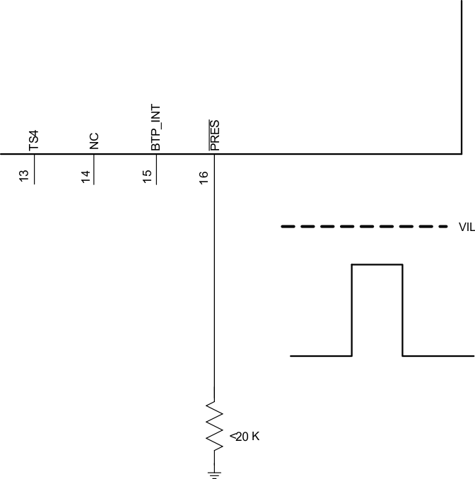
The system present signal informs the gas gauge whether the pack is installed into or removed from the system. In the host system, this pin is grounded. The PRES pin of the BQ40Z50-R2 device is occasionally sampled to test for system present. In ACTIVE mode, the PRES pin is pulsed every 250 ms for a duration of 5 ms (RHOEN is on), and just before it is turned off, the state of the PRES pin is checked to see if it is low or high. The average of the four measurements is used to determine if the PRES is asserted or not. In SLEEP mode, the PRES pin is pulsed every "Sleep Voltage Time," and the state of the PRES pin is determined. A resistor can be used to pull the signal low and the resistance must be 20 kΩ or lower to ensure that the test pulse is lower than the VIL limit. The pullup current source is typically 10 µA to 20 µA. When the PRES pin is not pulsed, the PRES pin is tied internally to VSS (RHOUT is on), and any pullup on the PRES pin will cause a battery drain when not charging. Refer to the PRES pin diagram in
 Figure 9-8 System Present Pull-Down Resistor
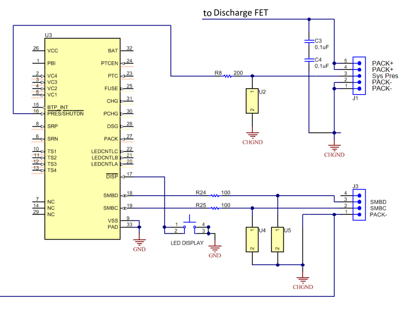
Because the System Present signal is part of the pack connector interface to the outside world, it must be protected from external electrostatic discharge events. The PRES pin has integrated ESD protection to 2 kV. External protection can be added to support higher ESD protection requirements. The TPD1E10B06 single-channel ESD protection diode (U2) can protect the input up to 30 kV, and the R8 reduces the holding current to release the internal SCR in the event that it triggers.
 Figure 9-9 System Present ESD and Short Protection