SLUSBS8B December 2013 – November 2019 BQ40Z50
PRODUCTION DATA.
- 1 Features
- 2 Applications
- 3 Description
- 4 Revision History
- 5 Description (continued)
- 6 Pin Configuration and Functions
-
7 Specifications
- 7.1 Absolute Maximum Ratings
- 7.2 ESD Ratings
- 7.3 Recommended Operating Conditions
- 7.4 Thermal Information
- 7.5 Electrical Characteristics: Supply Current
- 7.6 Electrical Characteristics: Power Supply Control
- 7.7 Electrical Characteristics: AFE Power-On Reset
- 7.8 Electrical Characteristics: AFE Watchdog Reset and Wake Timer
- 7.9 Electrical Characteristics: Current Wake Comparator
- 7.10 Electrical Characteristics: VC1, VC2, VC3, VC4, BAT, PACK
- 7.11 Electrical Characteristics: SMBD, SMBC
- 7.12 Electrical Characteristics: PRES, BTP_INT, DISP
- 7.13 Electrical Characteristics: LEDCNTLA, LEDCNTLB, LEDCNTLC
- 7.14 Electrical Characteristics: Coulomb Counter
- 7.15 Electrical Characteristics: CC Digital Filter
- 7.16 Electrical Characteristics: ADC
- 7.17 Electrical Characteristics: ADC Digital Filter
- 7.18 Electrical Characteristics: CHG, DSG FET Drive
- 7.19 Electrical Characteristics: PCHG FET Drive
- 7.20 Electrical Characteristics: FUSE Drive
- 7.21 Electrical Characteristics: Internal Temperature Sensor
- 7.22 Electrical Characteristics: TS1, TS2, TS3, TS4
- 7.23 Electrical Characteristics: PTC, PTCEN
- 7.24 Electrical Characteristics: Internal 1.8-V LDO
- 7.25 Electrical Characteristics: High-Frequency Oscillator
- 7.26 Electrical Characteristics: Low-Frequency Oscillator
- 7.27 Electrical Characteristics: Voltage Reference 1
- 7.28 Electrical Characteristics: Voltage Reference 2
- 7.29 Electrical Characteristics: Instruction Flash
- 7.30 Electrical Characteristics: Data Flash
- 7.31 Electrical Characteristics: OCD, SCC, SCD1, SCD2 Current Protection Thresholds
- 7.32 Timing Requirements: OCD, SCC, SCD1, SCD2 Current Protection Timing
- 7.33 Timing Requirements: SMBus
- 7.34 Timing Requirements: SMBus XL
- 7.35 Typical Characteristics
-
8 Detailed Description
- 8.1 Overview
- 8.2 Functional Block Diagram
- 8.3
Feature Description
- 8.3.1 Primary (1st Level) Safety Features
- 8.3.2 Secondary (2nd Level) Safety Features
- 8.3.3 Charge Control Features
- 8.3.4 Gas Gauging
- 8.3.5 Configuration
- 8.3.6 Battery Parameter Measurements
- 8.3.7 Battery Trip Point (BTP)
- 8.3.8 Lifetime Data Logging Features
- 8.3.9 Authentication
- 8.3.10 LED Display
- 8.3.11 Voltage
- 8.3.12 Current
- 8.3.13 Temperature
- 8.3.14 Communications
- 8.4 Device Functional Modes
- 9 Applications and Implementation
- 10Power Supply Recommendations
- 11Layout
- 12Device and Documentation Support
- 13Mechanical, Packaging, and Orderable Information
Package Options
Mechanical Data (Package|Pins)
- RSM|32
Thermal pad, mechanical data (Package|Pins)
- RSM|32
Orderable Information
9.2.2.1.4 Sense Resistor
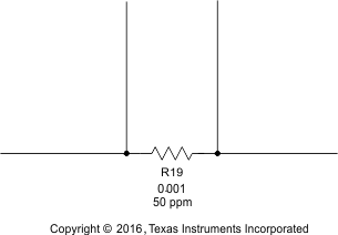
As with the cell connections, the quality of the Kelvin connections at the sense resistor is critical. The sense resistor must have a temperature coefficient no greater than 50 ppm in order to minimize current measurement drift with temperature. Choose the value of the sense resistor to correspond to the available overcurrent and short-circuit ranges of the BQ40Z50. Select the smallest value possible to minimize the negative voltage generated on the BQ40Z50 VSS node(s) during a short circuit. This pin has an absolute minimum of –0.3 V. Parallel resistors can be used as long as good Kelvin sensing is ensured. The device is designed to support a 1-mΩ to 3-mΩ sense resistor.
The ground scheme of BQ40Z50 is different from the older generation devices. In previous devices, the device ground (or low current ground) is connected to the SRN side of the Rsense resistor pad. The BQ40Z50, however, connects the low-current ground on the SRP side of the Rsense resistor pad, close to the battery 1N terminal (see Lithium-Ion Cell Connections). This is because the BQ40Z50 has one less VC pin (a ground reference pin VC5) compared to the previous devices. The pin was removed and was internally combined to SRP.
 Figure 25. Sense Resistor