SLUSBD6D July 2013 – July 2016
PRODUCTION DATA.
- 1 Features
- 2 Applications
- 3 Description
- 4 Revision History
- 5 Pin Configuration and Functions
- 6 Specifications
-
7 Detailed Description
- 7.1 Overview
- 7.2 Functional Block Diagram
- 7.3 Feature Description
- 7.4 Device Functional Modes
- 7.5 Programming
- 8 Application and Implementation
- 9 Power Supply Recommendations
- 10Layout
- 11Device and Documentation Support
- 12Mechanical, Packaging, and Orderable Information
Package Options
Mechanical Data (Package|Pins)
- RGZ|48
Thermal pad, mechanical data (Package|Pins)
- RGZ|48
Orderable Information
10 Layout
10.1 Layout Guidelines
A good PCB layout is critical to proper system operation. There are many references on proper PCB layout techniques.
Generally speaking, the system layout requires a 4-layer PCB layout, although a 2-layer PCB layout can be achieved. The following list is a proven and recommended approach to the layer stack-up:
- Layer 1, component placement and as much ground plane as possible
- Layer 2, clean ground
- Layer 3, finish routing
- Layer 4, clean ground
Thus, the circuitry is virtually sandwiched between grounds. This minimizes EMI noise emissions and also provides a noise free voltage reference plane for device operation.
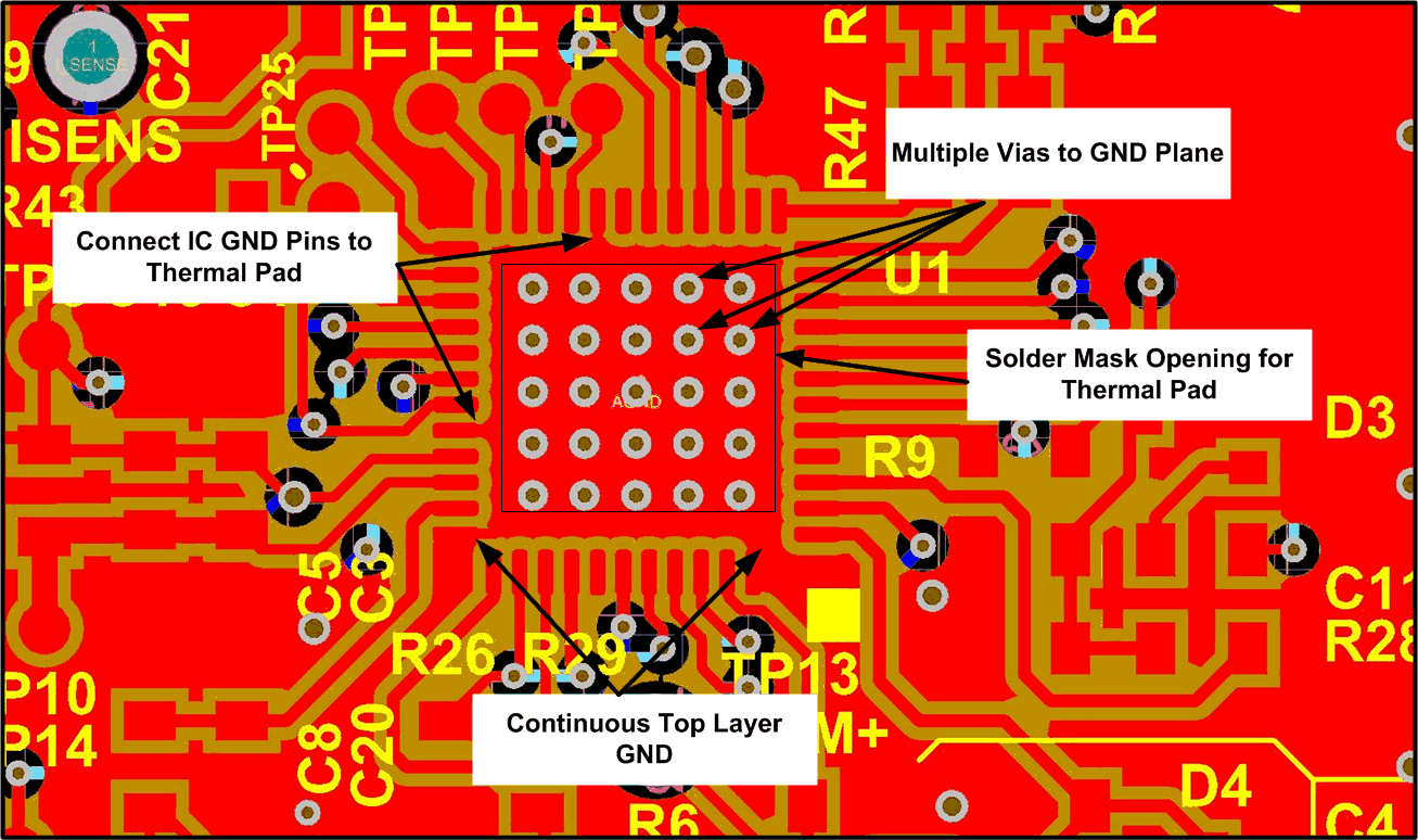
Keep as much copper as possible. Make sure the bq500212A GND pins and the power pad have a continuous flood connection to the ground plane. The power pad must also be stitched to the ground plane, which also acts as a heat sink for the bq500212A device. A good GND reference is necessary for proper bq500212A operation, such as analog-digital conversion, clock stability and best overall EMI performance.
Separate the analog ground plane from the power ground plane and use only one tie point to connect grounds. Having several tie points defeats the purpose of separating the grounds.
The COMM return signal from the resonant tank must be routed as a differential pair. This is intended to reduce stray noise induction. The frequencies of concern warrant low-noise analog signaling techniques, such as differential routing and shielding, but the COMM signal lines do not need to be impedance matched.
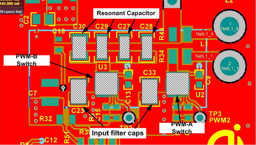
Typically a single-chip controller solution with integrated power FET and synchronous rectifier is used. To create a tight loop, pull in the buck inductor and power loop as close as possible. Likewise, the power train, full-bridge components must be pulled together as tight as possible. See the bq500212AEVM-550, bqTESLA Wireless Power TX EVM User's Guide (SLVU536) for layout examples.
Use a ground flood connection for the ground plane under the device. Connect the device ground pins to the thermal pad. Flow the ground plane between the thermal pad and top layer ground. Use multiple vias to connect the thermal pad to the internal ground layer. Verify that the solder mask under the device is removed for good connection to the thermal pad.
The customer must choose a full-bridge option to design the power section. Figure 13, based on the bq500212A EVM, uses a power stage device, which is an integrated drive and two MOSFETs.
10.2 Layout Example
 Figure 12. bq500212A IC Ground Connections
 Figure 13. bq500212A Power Section Using CSD9794Q4M or CSD97376Q4M Power Stage