SLUSBS9A February 2014 – July 2014
PRODUCTION DATA.
- 1 Features
- 2 Applications
- 3 Description
- 4 Simplified Schematic
- 5 Revision History
- 6 Device Comparison Table
- 7 Pin Configuration and Functions
- 8 Specifications
-
9 Detailed Description
- 9.1 Overview
- 9.2 Functional Block Diagram
- 9.3
Feature Description
- 9.3.1 Dynamic Rectifier Control
- 9.3.2 Dynamic Power Scaling
- 9.3.3 VO_REG and VIREG Calculations
- 9.3.4 RILIM Calculations
- 9.3.5 Adapter Enable Functionality
- 9.3.6 Turning Off the Transmitter
- 9.3.7 CM_ILIM
- 9.3.8 PD_DET and TMEM
- 9.3.9 TS, Both WPC and PMA
- 9.3.10 I2C Communication
- 9.3.11 Input Overvoltage
- 9.4 Device Functional Modes
- 9.5 Register Maps
-
10Application and Implementation
- 10.1 Application Information
- 10.2
Typical Applications
- 10.2.1
Dual Mode Design (WPC and PMA Compliant) Power Supply 5-V Output With 1-A Maximum Current
- 10.2.1.1 Design Requirements
- 10.2.1.2
Detailed Design Procedure
- 10.2.1.2.1 Output Voltage Set Point
- 10.2.1.2.2 Output and Rectifier Capacitors
- 10.2.1.2.3 Maximum Output Current Set Point
- 10.2.1.2.4 TERM Resistor
- 10.2.1.2.5 Setting LPRB1 and LPRB2 Resistors
- 10.2.1.2.6 I2C
- 10.2.1.2.7 Communication Current Limit
- 10.2.1.2.8 Receiver Coil
- 10.2.1.2.9 Series and Parallel Resonant Capacitors
- 10.2.1.2.10 Communication, Boot and Clamp Capacitors
- 10.2.1.3 Application Curves
- 10.2.2 bq51221 Embedded in System Board
- 10.2.3 bq51221 Implemented in Back Cover
- 10.2.1
Dual Mode Design (WPC and PMA Compliant) Power Supply 5-V Output With 1-A Maximum Current
- 11Power Supply Recommendations
- 12Layout
- 13Device and Documentation Support
- 14Mechanical, Packaging, and Orderable Information
Package Options
Mechanical Data (Package|Pins)
- YFP|42
Thermal pad, mechanical data (Package|Pins)
Orderable Information
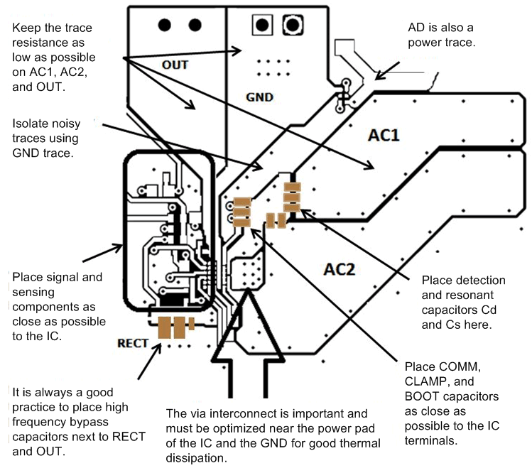
12 Layout
12.1 Layout Guidelines
- Keep the trace resistance as low as possible on AC1, AC2, and OUT.
- Detection and resonant capacitors need to be as close to the device as possible.
- COMM, CLAMP, and BOOT capacitors need to be placed as close to the device as possible.
- Via interconnect on GND net is critical for appropriate signal integrity and proper thermal performance.
- High frequency bypass capacitors need to be placed close to RECT and OUT pins.
- ILIM and FOD resistors are important signal paths and the loops in those paths to GND must be minimized.
- AC1 = AC2 = 1.2 A
- OUT = 1 A
- RECT = 100 mA (RMS)
- COMMx = 300 mA
- CLAMPx = 500 mA
- All others can be rated for 10 mA or less
Signal and sensing traces are the most sensitive to noise; the sensing signal amplitudes are usually measured in mV, which is comparable to the noise amplitude. Make sure that these traces are not being interfered by the noisy and power traces. AC1, AC2, BOOT1, BOOT2, COMM1, and COMM2 are the main source of noise in the board. These traces should be shielded from other components in the board. It is usually preferred to have a ground copper area placed underneath these traces to provide additional shielding. Also, make sure they do not interfere with the signal and sensing traces. The PCB should have a ground plane (return) connected directly to the return of all components through vias (two vias per capacitor for power-stage capacitors, one via per capacitor for small-signal components).
For a 1-A fast charge current application, the current rating for each net is as follows:
12.2 Layout Example