SLUSAX1L December 2012 – June 2021 BQ7718
PRODMIX
- 1 Features
- 2 Applications
- 3 Description
- 4 Revision History
- 5 Device Comparison Table
- 6 Pin Configuration and Functions
- 7 Specifications
- 8 Detailed Description
- 9 Application and Implementation
- 10Power Supply Recommendations
- 11Layout
- 12Device and Documentation Support
- 13Mechanical, Packaging, and Orderable Information
Package Options
Mechanical Data (Package|Pins)
- DPJ|8
Thermal pad, mechanical data (Package|Pins)
Orderable Information
8.3 Feature Description
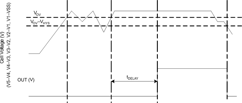
In the BQ7718xy device, each cell is monitored independently. Overvoltage is detected by comparing the actual cell voltage to a protection voltage reference, VOV. If any cell voltage exceeds the programmed OV value, a timer circuit is activated. When the timer expires, the OUT pin goes from inactive to active state.
For NCH Open Drain Active Low configurations, the OUT pin pulls down to VSS when active (OV present) and is high impedance when inactive (no OV).
 Figure 8-1 Timing for Overvoltage Sensing