SLUSC23 September 2015
PRODUCTION DATA.
- 1 Features
- 2 Applications
- 3 Description
- 4 Simplified Schematic
- 5 Revision History
- 6 Pin Configuration and Functions
-
7 Specifications
- 7.1 Absolute Maximum Ratings
- 7.2 ESD Ratings
- 7.3 Recommended Operating Conditions
- 7.4 Supply Current
- 7.5 Power Supply Control
- 7.6 Low-Voltage General Purpose I/O, TS1
- 7.7 Power-On Reset (POR)
- 7.8 Internal 1.8-V LDO
- 7.9 Current Wake Comparator
- 7.10 Coulomb Counter
- 7.11 ADC Digital Filter
- 7.12 ADC Multiplexer
- 7.13 Cell Balancing Support
- 7.14 Internal Temperature Sensor
- 7.15 NTC Thermistor Measurement Support
- 7.16 High-Frequency Oscillator
- 7.17 Low-Frequency Oscillator
- 7.18 Voltage Reference 1
- 7.19 Voltage Reference 2
- 7.20 Instruction Flash
- 7.21 Data Flash
- 7.22 Current Protection Thresholds
- 7.23 Current Protection Timing
- 7.24 N-CH FET Drive (CHG, DSG)
- 7.25 I2C and HDQ Interface I/O
- 7.26 I2C Interface Timing
- 7.27 HDQ Interface Timing
- 7.28 Typical Characteristics
-
8 Detailed Description
- 8.1 Overview
- 8.2 Functional Block Diagram
- 8.3
Feature Description
- 8.3.1 Battery Parameter Measurements
- 8.3.2 Coulomb Counter (CC)
- 8.3.3 CC Digital Filter
- 8.3.4 ADC Multiplexer
- 8.3.5 Analog-to-Digital Converter (ADC)
- 8.3.6 ADC Digital Filter
- 8.3.7 Internal Temperature Sensor
- 8.3.8 External Temperature Sensor Support
- 8.3.9 Power Supply Control
- 8.3.10 Power-On Reset
- 8.3.11 Bus Communication Interface
- 8.3.12 Cell Balancing Support
- 8.3.13 N-Channel Protection FET Drive
- 8.3.14 Low Frequency Oscillator
- 8.3.15 High Frequency Oscillator
- 8.3.16 1.8-V Low Dropout Regulator
- 8.3.17 Internal Voltage References
- 8.3.18 Overcurrent in Discharge Protection
- 8.3.19 Short-Circuit Current in Charge Protection
- 8.3.20 Short-Circuit Current in Discharge 1 and 2 Protection
- 8.3.21 Primary Protection Features
- 8.3.22 Gas Gauging
- 8.3.23 Charge Control Features
- 8.3.24 Authentication
- 8.4 Device Functional Modes
- 9 Applications and Implementation
- 10Power Supply Requirements
- 11Layout
- 12Device and Documentation Support
- 13Mechanical, Packaging, and Orderable Information
Package Options
Mechanical Data (Package|Pins)
- DRZ|12
Thermal pad, mechanical data (Package|Pins)
Orderable Information
8 Detailed Description
8.1 Overview
The bq78z100 gas gauge is a fully integrated battery manager that employs flash-based firmware and integrated hardware protection to provide a complete solution for battery-stack architectures composed of 1-series or 2-series cells. The bq78z100 device interfaces with a host system via I2C or HDQ protocols. High-performance, integrated analog peripherals enable support for a sense resistor down to 1 mΩ and simultaneous current/voltage data conversion for instant power calculations. The following sections detail all of the major component blocks included as part of the bq78z100 device.
8.2 Functional Block Diagram
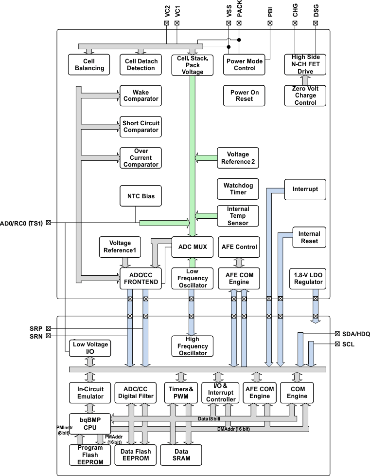
The Functional Block Diagram shows the analog and digital peripheral content in the bq78z100 device.

8.3 Feature Description
8.3.1 Battery Parameter Measurements
The bq78z100 device measures cell voltage and current simultaneously, and also measures temperature to calculate the information related to remaining capacity, full charge capacity, state-of-health, and other gauging parameters.
8.3.1.1 bq78z100 Processor
The bq78z100 device uses a custom TI-proprietary processor design that features a Harvard architecture and operates at frequencies up to 4.2 MHz. Using an adaptive, three-stage instruction pipeline, the bq78z100 processor supports variable instruction length of 8, 16, or 24 bits.
8.3.2 Coulomb Counter (CC)
The first ADC is an integrating converter designed specifically for coulomb counting. The converter resolution is a function of its full-scale range and number of bits, yielding a 3.74-µV resolution.
8.3.3 CC Digital Filter
The CC digital filter generates a 16-bit conversion value from the delta-sigma CC front-end. Its FIR filter uses the LFO clock output, which allows it to stop the HFO clock during conversions. New conversions are available every 250 ms while CCTL[CC_ON] = 1. Proper use of this peripheral requires turning on the CC modulator in the AFE.
8.3.4 ADC Multiplexer
The ADC multiplexer provides selectable connections to the VCx inputs, TS1 inputs, internal temperature sensor, internal reference voltages, internal 1.8-V regulator, PACK input, and VSS ground reference input. In addition, the multiplexer can independently enable the TS1 input connection to the internal thermistor biasing circuitry, and also enables the user to short the multiplexer inputs for test and calibration purposes.
8.3.5 Analog-to-Digital Converter (ADC)
The second ADC is a 16-bit delta-sigma converter designed for general-purpose measurements. The ADC automatically scales the input voltage range during sampling based on channel selection. The converter resolution is a function of its full-scale range and number of bits, yielding a 38-µV resolution. The default conversion time of the ADC is 31.25 ms, but is user-configurable down to 1.95 ms. Decreasing the conversion time presents a tradeoff between conversion speed and accuracy, as the resolution decreases for faster conversion times.
8.3.6 ADC Digital Filter
The ADC digital filter generates a 24-bit conversion result from the delta-sigma ADC front end. Its FIR filter uses the LFO clock, which allows it to stop the HFO clock during conversions. The ADC digital filter is capable of providing two 24-bit results: one result from the delta-sigma ADC front-end and a second synchronous result from the delta-sigma CC front-end.
8.3.7 Internal Temperature Sensor
An internal temperature sensor is available on the bq78z100 device to reduce the cost, power, and size of the external components necessary to measure temperature. It is available for connection to the ADC using the multiplexer, and is ideal for quickly determining pack temperature under a variety of operating conditions.
8.3.8 External Temperature Sensor Support
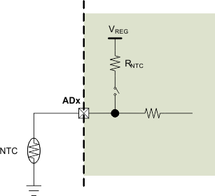
The TS1 input is enabled with an internal 18-kΩ (Typ.) linearization pull-up resistor to support the use of a 10-kΩ (25°C) NTC external thermistor, such as the Semitec 103AT-2. The NTC thermistor should be connected between VSS and the individual TS1 pin. The analog measurement is then taken via the ADC through its input multiplexer. If a different thermistor type is required, then changes to configurations may be required.
 Figure 19. External Thermistor Biasing
8.3.9 Power Supply Control
The bq78z100 device manages its supply voltage dynamically according to operating conditions. When VVC2 > VSWITCHOVER– + VHYS, the AFE connects an internal switch to BAT and uses this pin to supply power to its internal 1.8-V LDO, which subsequently powers all device logic and flash operations. Once VC2 decreases to VVC2 < VSWITCHOVER–, the AFE disconnects its internal switch from VC2 and connects another switch to PACK, allowing sourcing of power from a charger (if present). An external capacitor connected to PBI provides a momentary supply voltage to help guard against system brownouts due to transient short-circuit or overload events that pull VC2 below VSWITCHOVER–.
8.3.10 Power-On Reset
In the event of a power-cycle, the bq78z100 AFE holds its internal RESET output pin high for tRST duration to allow its internal 1.8-V LDO and LFO to stabilize before running the AGG. The AFE enters power-on reset when the voltage at VREG falls below VREGIT– and exits reset when VREG rises above VREGIT– + VHYS for tRST time. After tRST, the bq78z100 AGG will write its trim values to the AFE.
 Figure 20. POR Timing Diagram
8.3.11 Bus Communication Interface
The bq78z100 device has an I2C bus communication interface by default, but can be configured to use the single-wire HDQ interface. Devices for end applications that operate in HDQ mode are intended to be kept in default I2C mode as they go through pack manufacturer production line so that they can be configured and tested at the PCB level before they are converted to HDQ mode.
CAUTION
If the device is configured as a single-master architecture (an application processor) and an occasional NACK is detected in the operation, the master can resend the transaction. However, in a multi-master architecture, an incorrect ACK leading to accidental loss of bus arbitration can cause a master to wait incorrectly for another master to clear the bus. If this master does not get a bus-free signal, then it must have in place a method to look for the bus and assume it is free after some period of time. Also, if possible, set the clock speed to be 100 kHz or less to significantly reduce the issue described above for multi-mode operation.
8.3.12 Cell Balancing Support
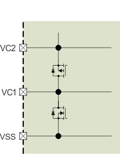
The integrated cell balancing FETs included in the bq78z100 device enable the AFE to bypass cell current around a given cell or numerous cells to effectively balance the entire battery stack. External series resistors placed between the cell connections and the VCx input pins set the balancing current magnitude. The cell balancing circuitry can be enabled or disabled via the CELL_BAL_DET[CB2, CB1] control register. Series input resistors between 100 Ω and 1 kΩ are recommended for effective cell balancing.
 Figure 21. Internal Cell Balancing
8.3.13 N-Channel Protection FET Drive
The bq78z100 device controls two external N-Channel MOSFETs in a back-to-back configuration for battery protection. The charge (CHG) and discharge (DSG) FETs are automatically disabled if a safety fault (AOLD, ASSC, ASCD, SOV) is detected, and can also be manually turned off using AFE_CONTROL[CHGEN, DSGEN] = 0, 0. When the gate drive is disabled, an internal circuit discharges CHG to VC2 and DSG to PACK.
8.3.14 Low Frequency Oscillator
The bq78z100 AFE includes a low frequency oscillator (LFO) running at 262.144 kHz. The AFE monitors the LFO frequency and indicates a failure via LATCH_STATUS[LFO] if the output frequency is much lower than normal.
8.3.15 High Frequency Oscillator
The bq78z100 AGG includes a high frequency oscillator (HFO) running at 16.78 MHz. It is synthesized from the LFO output and scaled down to 8.388 MHz with 50% duty cycle.
8.3.16 1.8-V Low Dropout Regulator
The bq78z100 AFE contains an integrated 1.8-V LDO that provides regulated supply voltage for the device CPU and internal digital logic.
8.3.17 Internal Voltage References
The bq78z100 AFE provides two internal voltage references with VREF1, used by the ADC and CC, while VREF2 is used by the LDO, LFO, current wake comparator, and OCD/SCC/SCD1/SCD2 current protection circuitry.
8.3.18 Overcurrent in Discharge Protection
The overcurrent in discharge (OCD) function detects abnormally high current in the discharge direction. The overload in discharge threshold and delay time are configurable via the OCD_CONTROL register. The thresholds and timing can be fine-tuned even further based on a sense resistor with lower resistance or wider tolerance via the PROTECTION_CONTROL register. The detection circuit also incorporates a filtered delay before disabling the CHG and DSG FETs. When an OCD event occurs, the LATCH_STATUS[OCD] bit is set to 1 and is latched until it is cleared and the fault condition has been removed.
8.3.19 Short-Circuit Current in Charge Protection
The short-circuit current in charge (SCC) function detects catastrophic current conditions in the charge direction. The short-circuit in charge threshold and delay time are configurable via the SCC_CONTROL register. The thresholds and timing can be fine-tuned even further based on a sense resistor with lower resistance or wider tolerance via the PROTECTION_CONTROL register. The detection circuit also incorporates a blanking delay before disabling the CHG and DSG FETs. When an SCC event occurs, the LATCH_STATUS[SCC] bit is set to 1 and is latched until it is cleared and the fault condition has been removed.
8.3.20 Short-Circuit Current in Discharge 1 and 2 Protection
The short-circuit current in discharge (SCD) function detects catastrophic current conditions in the discharge direction. The short-circuit in discharge thresholds and delay times are configurable via the SCD1_CONTROL and SCD2_CONTROL registers. The thresholds and timing can be fine-tuned even further based on a sense resistor with lower resistance or wider tolerance via the PROTECTION_CONTROL register. The detection circuit also incorporates a blanking delay before disabling the CHG and DSG FETs. When an SCD event occurs, the LATCH_STATUS[SCD1] or LATCH_STATUS[SCD2] bit is set to 1 and is latched until it is cleared and the fault condition has been removed.
8.3.21 Primary Protection Features
The bq78z100 gas gauge supports the following battery and system level protection features, which can be configured using firmware:
- Cell Undervoltage Protection
- Cell Overvoltage Protection
- Overcurrent in CHARGE Mode Protection
- Overcurrent in DISCHARGE Mode Protection
- Overload in DISCHARGE Mode Protection
- Short Circuit in CHARGE Mode Protection
- Overtemperature in CHARGE Mode Protection
- Overtemperature in DISCHARGE Mode Protection
- Precharge Timeout Protection
- Fast Charge Timeout Protection
8.3.22 Gas Gauging
This device uses the Impedance Track technology to measure and determine the available charge in battery cells. The accuracy achieved using this method is better than 1% error over the lifetime of the battery. There is no full charge/discharge learning cycle required. See the Theory and Implementation of Impedance Track Battery Fuel-Gauging Algorithm Application Report (SLUA364B) for further details.
8.3.23 Charge Control Features
This device supports charge control features, such as:
- Reports charging voltage and charging current based on the active temperature range—JEITA temperature ranges T1, T2, T3, T4, T5, and T6
- Provides more complex charging profiles, including sub-ranges within a standard temperature range
- Reports the appropriate charging current required for constant current charging and the appropriate charging voltage needed for constant voltage charging to a smart charger, using the bus communication interface
- Selects the chemical state-of-charge of each battery cell using the Impedance Track method, and reduces the voltage difference between cells when cell balancing multiple cells in a series
- Provides pre-charging/zero-volt charging
- Employs charge inhibit and charge suspend if battery pack temperature is out of programmed range
- Reports charging faults and indicates charge status via charge and discharge alarms
8.3.24 Authentication
This device supports security by:
- Authentication by the host using the SHA-1 method
- The gas gauge requires SHA-1 authentication before the device can be unsealed or allow full access.
8.4 Device Functional Modes
This device supports three modes, but the current consumption varies, based on firmware control of certain functions and modes of operation:
- NORMAL mode: In this mode, the device performs measurements, calculations, protections, and data updates every 250-ms intervals. Between these intervals, the device is operating in a reduced power stage to minimize total average current consumption.
- SLEEP mode: In this mode, the device performs measurements, calculations, protections, and data updates in adjustable time intervals. Between these intervals, the device is operating in a reduced power stage to minimize total average current consumption.
- SHUTDOWN mode: The device is completely disabled.
8.4.1 Lifetime Logging Features
The device supports data logging of several key parameters for warranty and analysis:
- Maximum and Minimum Cell Temperature
- Maximum Current in CHARGE or DISCHARGE Mode
- Maximum and Minimum Cell Voltages
8.4.2 Configuration
The device supports accurate data measurements and data logging of several key parameters.
8.4.2.1 Coulomb Counting
The device uses an integrating delta-sigma analog-to-digital converter (ADC) for current measurement. The ADC measures charge/discharge flow of the battery by measuring the voltage across a very small external sense resistor. The integrating ADC measures a bipolar signal from a range of –100 mV to 100 mV, with a positive value when V(SRP) – V(SRN), indicating charge current and a negative value indicating discharge current. The integration method uses a continuous timer and internal counter, which has a rate of 0.65 nVh.
8.4.2.2 Cell Voltage Measurements
The bq78z100 measures the individual cell voltages at 250-ms intervals using an ADC. This measured value is internally scaled for the ADC and is calibrated to reduce any errors due to offsets. This data is also used for calculating the impedance of the individual cell for Impedance Track gas gauging.
8.4.2.3 Current Measurements
The current measurement is performed by measuring the voltage drop across the external sense resistor (1 mΩ to 3 mΩ) and the polarity of the differential voltage determines if the cell is in the CHARGE or DISCHARGE mode.
8.4.2.4 Auto Calibration
The auto-calibration feature helps to cancel any voltage offset across the SRP and SRN pins for accurate measurement of the cell voltage, charge/discharge current, and thermistor temperature. The auto-calibration is performed when there is no communication activity for a minimum of 5 s on the bus lines.
8.4.2.5 Temperature Measurements
This device has an internal sensor for on-die temperature measurements, and the ability to support external temperature measurements via the external NTC on the TS1 pin. These two measurements are individually enabled and configured.