SWAS037B February   2019  – May 2021 CC3135

PRODUCTION DATA  

  1. Features
  2. Applications
  3. Description
  4. Functional Block Diagram
  5. Revision History
  6. Device Comparison
    1. 6.1 Related Products
  7. Terminal Configuration and Functions
    1. 7.1 Pin Diagram
    2. 7.2 Pin Attributes
    3. 7.3 Signal Descriptions
      1.      12
    4. 7.4 Connections for Unused Pins
  8. Specifications
    1. 8.1  Absolute Maximum Ratings
    2. 8.2  ESD Ratings
    3. 8.3  Power-On Hours (POH)
    4. 8.4  Recommended Operating Conditions
    5. 8.5  Current Consumption Summary: 2.4 GHz RF Band
    6. 8.6  Current Consumption Summary: 5 GHz RF Band
    7. 8.7  TX Power Control for 2.4 GHz Band
    8. 8.8  TX Power Control for 5 GHz
    9. 8.9  Brownout and Blackout Conditions
      1.      24
    10. 8.10 Electrical Characteristics for DIO Pins
      1.      26
      2.      27
    11. 8.11 Electrical Characteristics for Pin Internal Pullup and Pulldown
    12. 8.12 WLAN Receiver Characteristics
      1.      30
      2.      31
    13. 8.13 WLAN Transmitter Characteristics
      1.      33
      2.      34
    14. 8.14 WLAN Transmitter Out-of-Band Emissions
      1.      36
      2.      37
    15. 8.15 BLE/2.4 GHz Radio Coexistence and WLAN Coexistence Requirements
    16. 8.16 Thermal Resistance Characteristics for RGK Package
    17. 8.17 Timing and Switching Characteristics
      1. 8.17.1 Power Supply Sequencing
      2. 8.17.2 Device Reset
      3. 8.17.3 Reset Timing
        1. 8.17.3.1 nRESET (32-kHz Crystal)
        2.       45
        3. 8.17.3.2 nRESET (External 32-kHz Crystal)
          1.        47
      4. 8.17.4 Wakeup From HIBERNATE Mode
        1.       49
      5. 8.17.5 Clock Specifications
        1. 8.17.5.1 Slow Clock Using Internal Oscillator
          1.        52
        2. 8.17.5.2 Slow Clock Using an External Clock
          1.        54
        3. 8.17.5.3 Fast Clock (Fref) Using an External Crystal
          1.        56
        4. 8.17.5.4 Fast Clock (Fref) Using an External Oscillator
          1.        58
      6. 8.17.6 Interfaces
        1. 8.17.6.1 Host SPI Interface Timing
          1.        61
        2. 8.17.6.2 Flash SPI Interface Timing
          1.        63
        3. 8.17.6.3 DIO Interface Timing
          1. 8.17.6.3.1 DIO Output Transition Time Parameters (Vsupply = 3.3 V)
            1.         66
          2. 8.17.6.3.2 DIO Input Transition Time Parameters
            1.         68
    18. 8.18 External Interfaces
      1. 8.18.1 SPI Flash Interface
      2. 8.18.2 SPI Host Interface
      3. 8.18.3 Host UART Interface
        1. 8.18.3.1 5-Wire UART Topology
        2. 8.18.3.2 4-Wire UART Topology
        3. 8.18.3.3 3-Wire UART Topology
  9. Detailed Description
    1. 9.1 Overview
    2. 9.2 Device Features
      1. 9.2.1 WLAN
      2. 9.2.2 Network Stack
      3. 9.2.3 Security
      4. 9.2.4 Host Interface and Driver
      5. 9.2.5 System
    3. 9.3 FIPS 140-2 Level 1 Certification
    4. 9.4 Power-Management Subsystem
      1. 9.4.1 VBAT Wide-Voltage Connection
    5. 9.5 Low-Power Operating Modes
      1. 9.5.1 Low-Power Deep Sleep
      2. 9.5.2 Hibernate
      3. 9.5.3 Shutdown
    6. 9.6 Memory
      1. 9.6.1 External Memory Requirements
    7. 9.7 Restoring Factory Default Configuration
    8. 9.8 Hostless Mode
  10. 10Applications, Implementation, and Layout
    1. 10.1 Application Information
      1. 10.1.1 BLE/2.4 GHz Radio Coexistence
      2. 10.1.2 Antenna Selection
      3. 10.1.3 Typical Application
    2. 10.2 PCB Layout Guidelines
      1. 10.2.1 General PCB Guidelines
      2. 10.2.2 Power Layout and Routing
        1. 10.2.2.1 Design Considerations
      3. 10.2.3 Clock Interface Guidelines
      4. 10.2.4 Digital Input and Output Guidelines
      5. 10.2.5 RF Interface Guidelines
  11. 11Device and Documentation Support
    1. 11.1  Third-Party Products Disclaimer
    2. 11.2  Tools and Software
    3. 11.3  Firmware Updates
    4. 11.4  Device Nomenclature
    5. 11.5  Documentation Support
    6. 11.6  Support Resources
    7. 11.7  Trademarks
    8. 11.8  Electrostatic Discharge Caution
    9. 11.9  Export Control Notice
    10. 11.10 Glossary
  12. 12Mechanical, Packaging, and Orderable Information
    1. 12.1 Packaging Information
    2. 12.2 Package Option Addendum
      1. 12.2.1 Packaging Information
      2. 12.2.2 Tape and Reel Information

Package Options

Mechanical Data (Package|Pins)
Thermal pad, mechanical data (Package|Pins)
Orderable Information

Fast Clock (Fref) Using an External Oscillator

The CC3135 device can accept an external TCXO/XO for the 40-MHz clock. In this mode of operation, the clock is connected to WLAN_XTAL_P (pin 23). WLAN_XTAL_N (pin 22) is connected to GND. The external TCXO/XO can be enabled by TCXO_EN (pin 21) from the device to optimize the power consumption of the system.

If the TCXO does not have an enable input, an external LDO with an enable function can be used. Using the LDO improves noise on the TCXO power supply.

Figure 8-12 shows the connection.
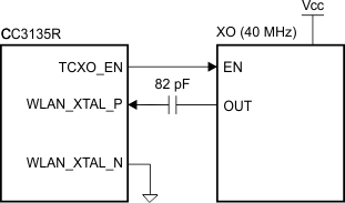
GUID-D4EBC38B-9FD4-4BE8-8937-5066A4ABC6E8-low.gifFigure 8-12 External TCXO Input


Table 8-17 lists the external Fref clock requirements.