SCHS032D November 1998 – July 2021 CD4027B
PRODUCTION DATA
- 1 Features
- 2 Applications
- 3 Description
- 4 Revision History
- 5 Pin Configuration and Functions
- 6 Specifications
- 7 Parameter Measurement Information
- 8 Detailed Description
- 9 Device and Documentation Support
- 10Mechanical, Packaging, and Orderable Information
Package Options
Refer to the PDF data sheet for device specific package drawings
Mechanical Data (Package|Pins)
- J|16
Thermal pad, mechanical data (Package|Pins)
Orderable Information
3 Description
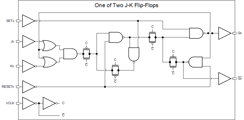
CD4027B is a single monolithic chip integrated circuit containing two identical complementary-symmetry J-K flip flops. Each flip-flop has provisions for individual J, K, Set, Reset, and Clock input signals. Buffered Q and Q signals are provided as outputs. This input-output arrangement provides for compatibile operation with the RCA-CD4013B dual D-type flip-flop.
The CD4027B is useful in performing control, register, and toggle functions. Logic levels present at the J and K inputs along with internal self-steering control the state of each flip-flop; changes in the flip-flop state are synchronous with the postitive-going transition of the clock pulse. Set and reset functions are independent of the clock and are initiated when a high level signal is present at either the Set or Reset input.
The CD4027B types are supplied in 16-lead hermetic dual-in-line ceramic packages (F3A suffix), 16-lead dual-in-line plastic packages (E suffice), 16-lead small-outline packages (M, M96, MT, and NSR suffixes), and 16-lead thin shrink small-outline packages (PW and PWR suffixes).
 Figure 3-1 Logic Diagram