SCHS158F November 1998 – March 2022 CD54HC173 , CD54HCT173 , CD74HC173 , CD74HCT173
PRODUCTION DATA
- 1 Features
- 2 Description
- 3 Revision History
- 4 Pin Configuration and Functions
- 5 Specifications
- 6 Parameter Measurement Information
- 7 Detailed Description
- 8 Power Supply Recommendations
- 9 Layout
- 10Device and Documentation Support
- 11Mechanical, Packaging, and Orderable Information
Package Options
Refer to the PDF data sheet for device specific package drawings
Mechanical Data (Package|Pins)
- PW|16
- N|16
- D|16
Thermal pad, mechanical data (Package|Pins)
- D|16
Orderable Information
6 Parameter Measurement Information
tPD is the maximum between tPLH and tPHL
tt is the maximum between tTLH and tTHL
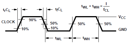
NOTE: Outputs should be switching from 10% VCC to 90% VCC in accordance with device truth table. For fMAX, input duty cycle = 50%
Figure 6-1 HC clock pulse rise and fall times and pulse width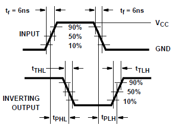 Figure 6-3 HC and HCU transition
times and propagation delay times, combination logic
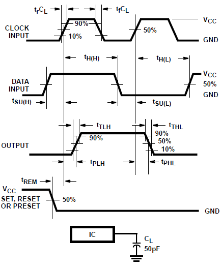 Figure 6-5 HC setup times, hold
times, removal time, and propagation delay times for edge triggered
sequential logic circuits
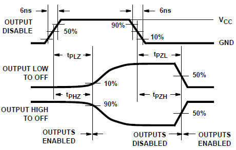 Figure 6-7 HC three-state propagation
delay waveform
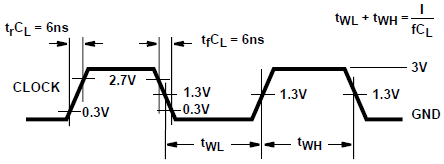
NOTE: Outputs should be switching from 10% VCC to 90% VCC in accordance with device truth table. FOr fMAX, input duty cycle = 50%
Figure 6-2 HCT clock pulse rise and fall times and pulse width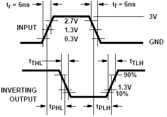 Figure 6-4 HCT transition times and
propagation delay times, combination logic
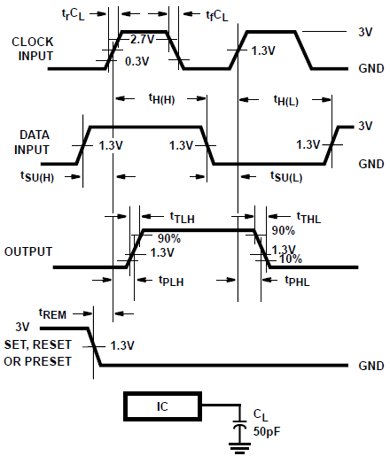 Figure 6-6 HCT setup times, hold
times, removal time, and propagation delay times for edge triggered
sequential logic circuits
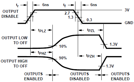 Figure 6-8 HCT three-state
propagation delay waveform
NOTE: Opend drain waveforms tPLZ and tPZL are the same as those for three-state shown on the left. The test circuit is Output RL = 1kΩ to VCC, CL = 50pF
Figure 6-9 HC and HCT three-state propagation delay test circuit