SCHS197F August 1997 – February 2022 CD54HC4002 , CD74HC4002
PRODUCTION DATA
- 1 Features
- 2 Description
- 3 Revision History
- 4 Pin Configuration and Functions
- 5 Specifications
- 6 Parameter Measurement Information
- 7 Detailed Description
- 8 Power Supply Recommendations
- 9 Layout
- 10Device and Documentation Support
- 11Mechanical, Packaging, and Orderable Information
Package Options
Refer to the PDF data sheet for device specific package drawings
Mechanical Data (Package|Pins)
- D|14
- PW|14
- N|14
Thermal pad, mechanical data (Package|Pins)
- D|14
Orderable Information
2 Description
The ’HC4002 logic gate utilizes silicon gate CMOS technology to achieve operating speeds similar to LSTTL gates with the low power consumption of standard CMOS integrated circuits. All devices have the ability to drive 10 LSTTL loads. The ’HC4002 logic family is functional as well as pin compatible with the standard LS logic family.
| PART NUMBER | PACKAGE(1) | BODY SIZE (NOM) |
|---|---|---|
| CD74HC4002M | SOIC (14) | 8.65 mm × 3.9 mm |
| CD54HC4002F3A | CDIP (14) | 19.55 mm × 6.71 mm |
| CD74HC4002E | PDIP (14) | 19.31 mm × 6.35 mm |
| CD74HC4002PW | TSSOP (14) | 5.0 mm × 4.4 mm |
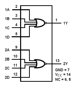
 Functional Block
Diagram