SCHS169D November 1998 – March 2022 CD54HC251 , CD54HCT251 , CD74HC251 , CD74HCT251
PRODUCTION DATA
- 1 Features
- 2 Description
- 3 Revision History
- 4 Pin Configuration and Functions
- 5 Specifications
- 6 Parameter Measurement Information
- 7 Detailed Description
- 8 Power Supply Recommendations
- 9 Layout
- 10Device and Documentation Support
- 11Mechanical, Packaging, and Orderable Information
Package Options
Refer to the PDF data sheet for device specific package drawings
Mechanical Data (Package|Pins)
- N|16
- D|16
Thermal pad, mechanical data (Package|Pins)
- D|16
Orderable Information
2 Description
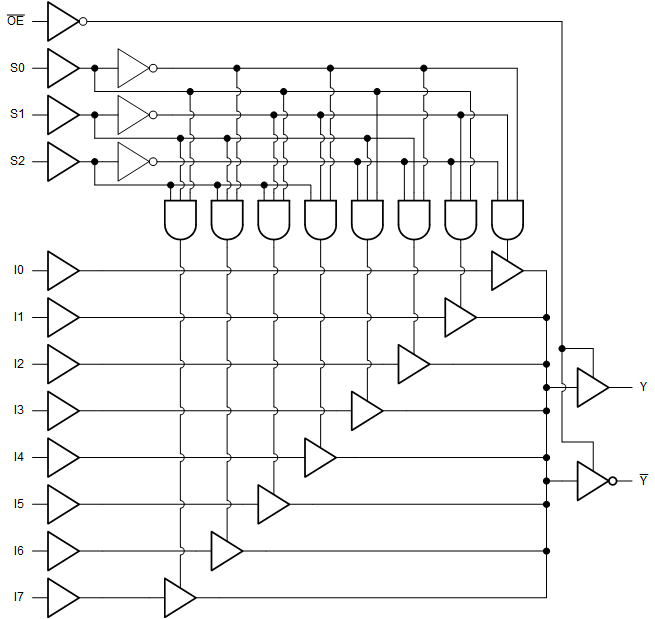
The ’HC251 and ’HCT251 are 8-channel digital multiplexers with three-state outputs, fabricated with high-speed silicongate CMOS technology. Together with the low power consumption of standard CMOS integrated circuits, they possess the ability to drive 10 LSTTL loads. The three-state feature makes them ideally suited for interfacing with bus lines in a bus-oriented system.
Device
Information
| PART NUMBER | PACKAGE(1) | BODY SIZE (NOM) |
|---|---|---|
| CD54HC251F | CDIP (16) | 24.38 mm × 6.92 mm |
| CD54HCT251F | CDIP (16) | 24.38 mm × 6.92 mm |
| CD74HC251M | SOIC (16) | 9.90 mm × 3.90 mm |
| CD74HCT251M | SOIC (16) | 9.90 mm × 3.90 mm |
| CD74HC251E | PDIP (16) | 19.31 mm × 6.35 mm |
| CD74HCT251E | PDIP (16) | 19.31 mm × 6.35 mm |
(1) For all
available packages, see the orderable addendum at the end of the data
sheet.
 Functional Block Diagram