SCHS211F November 1997 – March 2022 CD54HC4094 , CD74HC4094 , CD74HCT4094
PRODUCTION DATA
- 1 Features
- 2 Description
- 3 Revision History
- 4 Pin Configuration and Functions
- 5 Specifications
- 6 Parameter Measurement Information
- 7 Detailed Description
- 8 Power Supply Recommendations
- 9 Layout
- 10Device and Documentation Support
- 11Mechanical, Packaging, and Orderable Information
Package Options
Refer to the PDF data sheet for device specific package drawings
Mechanical Data (Package|Pins)
- N|16
- D|16
Thermal pad, mechanical data (Package|Pins)
- D|16
Orderable Information
2 Description
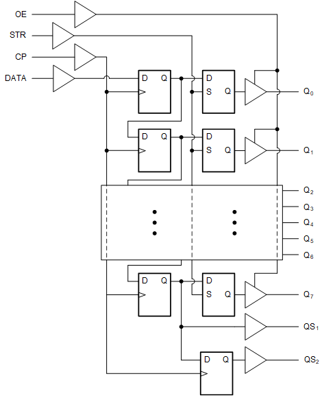
The CDx4HC4094 and CD74HCT4094 are 8-stage serial shift registers having a storage latch associated with each stage for strobing data from the serial input to parallel buffered tri-state outputs. The parallel outputs may be connected directly to common bus lines. Data is shifted on positive clock transitions. The data in each shift register stage is transferred to the storage register when the Strobe input is high. Data in the storage register appears at the outputs whenever the Output-Enable signal is high.
| PART NUMBER | PACKAGE(1) | BODY SIZE (NOM) |
|---|---|---|
| CD54HC4094F3A | CDIP (16) | 24.38 mm × 6.92 mm |
| CD74HC4094M | SOIC (16) | 9.90 mm × 3.90 mm |
| CD74HC4094E | PDIP (16) | 19.31 mm × 6.35 mm |
| CD74HC4094NSR | SO (16) | 6.20 mm × 5.30 mm |
| CD74HC4094PW | TSSOP (16) | 5.00 mm × 4.40 mm |
| CD74HCT4094M | SOIC (16) | 9.90 mm × 3.90 mm |
| CD74HCT4094E | PDIP (16) | 19.31 mm × 6.35 mm |
 Functional Block
Diagram