SCAS759C April 2004 – July 2017 CDCM1802
PRODUCTION DATA.
- 1 Features
- 2 Applications
- 3 Description
- 4 Revision History
- 5 Pin Configuration and Functions
-
6 Specifications
- 6.1 Absolute Maximum Ratings
- 6.2 ESD Ratings
- 6.3 Recommended Operating Conditions
- 6.4 Thermal Information
- 6.5 Electrical Characteristics
- 6.6 Switching Characteristics
- 6.7 Jitter Characteristics
- 6.8 Supply Current Electrical Characteristics
- 6.9 Control Input Characteristics
- 6.10 Timing Requirements
- 6.11 Bias Voltage VBB
- 6.12 Typical Characteristics
- 7 Parameter Measurement Information
- 8 Detailed Description
- 9 Application and Implementation
- 10Power Supply Recommendations
- 11Layout
- 12Device and Documentation Support
- 13Mechanical, Packaging, and Orderable Information
Package Options
Mechanical Data (Package|Pins)
- RGT|16
Thermal pad, mechanical data (Package|Pins)
- RGT|16
Orderable Information
7 Parameter Measurement Information

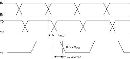
A. Part-to-part skew, tsk(pp), is calculated as the greater of:
M− The difference between the fastest and the slowest tpd(LH)n across multiple devices
M− The difference between the fastest and the slowest tpd(HL)n across multiple devices
M− The difference between the fastest and the slowest tpd(LH)n across multiple devices
M− The difference between the fastest and the slowest tpd(HL)n across multiple devices
B. Pulse skew, tsk(p), is calculated as the magnitude of the absolute time difference between the high-to-low (tpd(HL) and the low-to-high (tpd(LH)) propagation delays when a single switching input causes Y0 to switch,
tsk(p) = | tpd(HL) − tpd(LH) |. Pulse skew is sometimes referred to as pulse width distortion or duty cycle skew.
Figure 7. Waveforms for Calculation of tsk(o) and tsk(pp)
tsk(p) = | tpd(HL) − tpd(LH) |. Pulse skew is sometimes referred to as pulse width distortion or duty cycle skew.
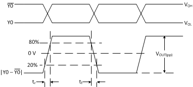
 Figure 8. LVPECL Differential Output Voltage and Rise and Fall Time
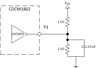
 Figure 9. LVCMOS Output Loading During Device Test
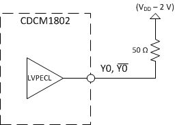
 Figure 10. LVPECL Output Loading During Device Test