SLPS530 January 2015 CSD19534KCS
PRODUCTION DATA.
- 1Features
- 2Applications
- 3Description
- 4Revision History
- 5Specifications
- 6Device and Documentation Support
- 7Mechanical, Packaging, and Orderable Information
Package Options
Refer to the PDF data sheet for device specific package drawings
Mechanical Data (Package|Pins)
- KCS|3
Thermal pad, mechanical data (Package|Pins)
Orderable Information
5 Specifications
5.1 Electrical Characteristics
(TA = 25°C unless otherwise stated)| PARAMETER | TEST CONDITIONS | MIN | TYP | MAX | UNIT | ||
|---|---|---|---|---|---|---|---|
| STATIC CHARACTERISTICS | |||||||
| BVDSS | Drain-to-Source Voltage | VGS = 0 V, ID = 250 μA | 100 | V | |||
| IDSS | Drain-to-Source Leakage Current | VGS = 0 V, VDS = 80 V | 1 | μA | |||
| IGSS | Gate-to-Source Leakage Current | VDS = 0 V, VGS = 20 V | 100 | nA | |||
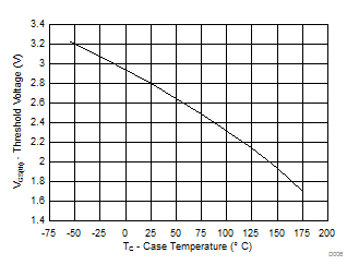
| VGS(th) | Gate-to-Source Threshold Voltage | VDS = VGS, ID = 250 μA | 2.4 | 2.8 | 3.4 | V | |
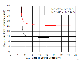
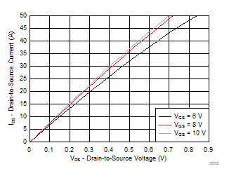
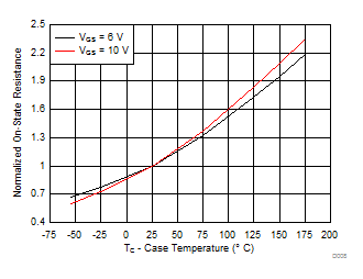
| RDS(on) | Drain-to-Source On-Resistance | VGS = 6 V, ID = 30 A | 16.3 | 20.0 | mΩ | ||
| VGS = 10 V, ID = 30 A | 13.7 | 16.5 | mΩ | ||||
| gƒs | Transconductance | VDS = 10 V, ID = 30 A | 80 | S | |||
| DYNAMIC CHARACTERISTICS | |||||||
| Ciss | Input Capacitance | VGS = 0 V, VDS = 50 V, ƒ = 1 MHz | 1290 | 1670 | pF | ||
| Coss | Output Capacitance | 257 | 334 | pF | |||
| Crss | Reverse Transfer Capacitance | 5.7 | 7.4 | pF | |||
| RG | Series Gate Resistance | 1.1 | 2.2 | Ω | |||
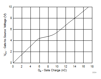
| Qg | Gate Charge Total (10 V) | VDS = 50 V, ID = 30 A | 17.1 | 22.2 | nC | ||
| Qgd | Gate Charge Gate-to-Drain | 3.2 | nC | ||||
| Qgs | Gate Charge Gate-to-Source | 5.1 | nC | ||||
| Qg(th) | Gate Charge at Vth | 3.3 | nC | ||||
| Qoss | Output Charge | VDS = 50 V, VGS = 0 V | 44 | nC | |||
| td(on) | Turn On Delay Time | VDS = 50 V, VGS = 10 V, IDS = 30 A, RG = 0 Ω |
6 | ns | |||
| tr | Rise Time | 2 | ns | ||||
| td(off) | Turn Off Delay Time | 9 | ns | ||||
| tƒ | Fall Time | 1 | ns | ||||
| DIODE CHARACTERISTICS | |||||||
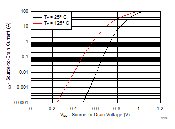
| VSD | Diode Forward Voltage | ISD = 30 A, VGS = 0 V | 0.9 | 1.1 | V | ||
| Qrr | Reverse Recovery Charge | VDS= 50 V, IF = 30 A, di/dt = 300 A/μs |
195 | nC | |||
| trr | Reverse Recovery Time | 72 | ns | ||||
5.2 Thermal Information
(TA = 25°C unless otherwise stated)| THERMAL METRIC | MIN | TYP | MAX | UNIT | |
|---|---|---|---|---|---|
| RθJC | Junction-to-Case Thermal Resistance | 1.3 | °C/W | ||
| RθJA | Junction-to-Ambient Thermal Resistance | 62 | |||
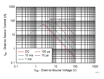
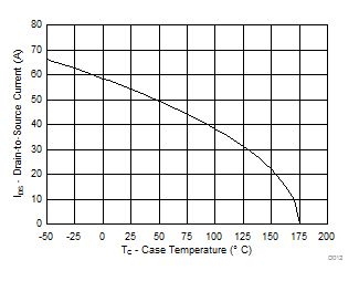
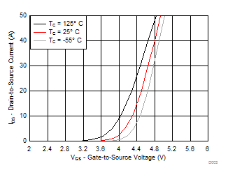
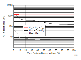
5.3 Typical MOSFET Characteristics
(TA = 25°C unless otherwise stated)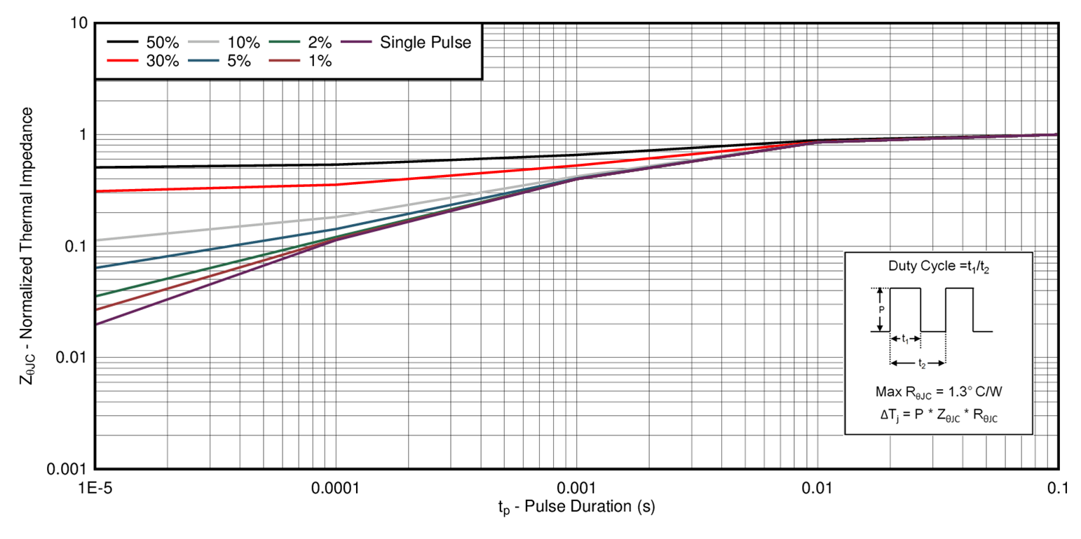 Figure 1. Transient Thermal Impedance
| ID = 30 A | VDS = 50 V | |
| ID = 250 µA | ||
| ID = 30 A | ||