SLPS431B June 2013 – December 2014 CSD22202W15
PRODUCTION DATA.
- 1Features
- 2Applications
- 3Description
- 4Revision History
- 5Specifications
- 6Device and Documentation Support
- 7Mechanical, Packaging, and Orderable Information
Package Options
Refer to the PDF data sheet for device specific package drawings
Mechanical Data (Package|Pins)
- YZF|9
Thermal pad, mechanical data (Package|Pins)
Orderable Information
7 Mechanical, Packaging, and Orderable Information
The following pages include mechanical, packaging, and orderable information. This information is the most current data available for the designated devices. This data is subject to change without notice and revision of this document. For browser-based versions of this data sheet, refer to the left-hand navigation.
7.1 CSD22202W15 Package Dimensions
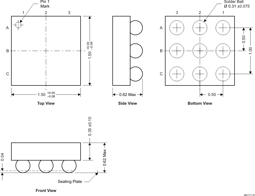
All dimensions are in mm (unless otherwise specified)
Table 1. Pinout
| POSITION | DESIGNATION |
|---|---|
| A1 | Gate |
| A2, A3, B1, B2, B3 | Source |
| C1, C2, C3 | Drain |
7.2 Recommended Land Pattern
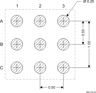
All dimensions are in mm (unless otherwise specified)
7.3 Tape and Reel Information
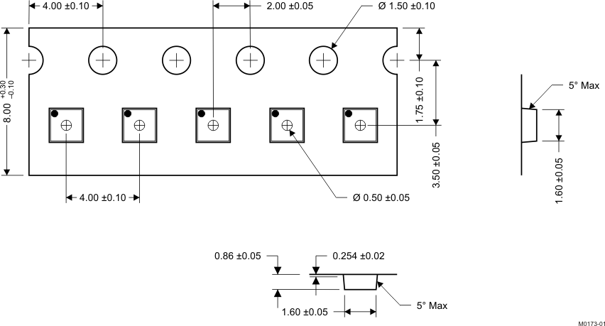
1. 10-sprocket hole-pitch cumulative tolerance ±0.2
2. Camber not to exceed 1 mm in 100 mm, noncumulative over 250 mm
3. Material: black static-dissipative polystyrene
4. All dimensions are in mm (unless otherwise specified).
5. Thickness: 0.30 ±0.05 mm
6. MSL1 260°C (IR and convection) PbF-reflow compatible