SLPS327B September 2012 – April 2018 CSD86360Q5D
PRODUCTION DATA.
- 1Features
- 2Applications
- 3Description
- 4Revision History
- 5Specifications
- 6Application and Implementation
- 7Layout
- 8Device and Documentation Support
- 9Mechanical, Packaging, and Orderable Information
Package Options
Mechanical Data (Package|Pins)
- DQY|8
Thermal pad, mechanical data (Package|Pins)
Orderable Information
6.1.1 Equivalent System Performance
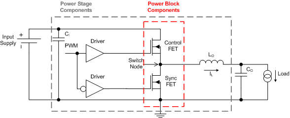
Many of today’s high-performance computing systems require low-power consumption in an effort to reduce system operating temperatures and improve overall system efficiency. This has created a major emphasis on improving the conversion efficiency of today’s synchronous buck topology. In particular, there has been an emphasis in improving the performance of the critical power semiconductor in the power stage of this application (see Figure 28). As such, optimization of the power semiconductors in these applications, needs to go beyond simply reducing RDS(ON).
 Figure 28. Equivalent System Schematic
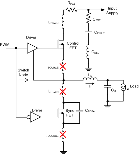
The CSD86360Q5D is part of TI’s power block product family, which is a highly optimized product for use in a synchronous buck topology requiring high current, high efficiency, and high frequency. It incorporates TI’s latest generation silicon, which has been optimized for switching performance, as well as minimizing losses associated with QGD, QGS, and QRR. Furthermore, TI’s patented packaging technology has minimized losses by nearly eliminating parasitic elements between the control FET and sync FET connections (see Figure 29). A key challenge solved by TI’s patented packaging technology is the system level impact of Common Source Inductance (CSI). CSI greatly impedes the switching characteristics of any MOSFET, which in turn increases switching losses and reduces system efficiency. As a result, the effects of CSI need to be considered during the MOSFET selection process. In addition, standard MOSFET switching loss equations used to predict system efficiency need to be modified in order to account for the effects of CSI. Further details behind the effects of CSI and modification of switching loss equations are outlined in Power Loss Calculation With CSI Consideration for Synchronous Buck Converters (SLPA009).
 Figure 29. Elimination of Parasitic Inductances
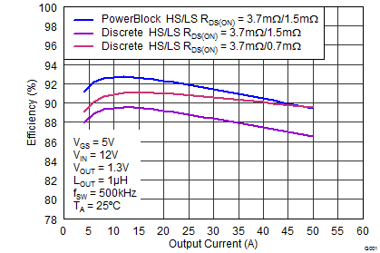
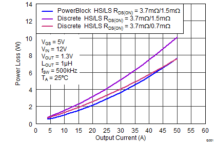
The combination of TI’s latest generation silicon and optimized packaging technology has created a benchmarking solution that outperforms industry standard MOSFET chipsets of similar RDS(ON) and MOSFET chipsets with lower RDS(ON). Figure 30 and Figure 31 compare the efficiency and power loss performance of the CSD86360Q5D versus industry standard MOSFET chipsets commonly used in this type of application. This comparison purely focuses on the efficiency and generated loss of the power semiconductors only. The performance of CSD86360Q5D clearly highlights the importance of considering the effective AC on-impedance (ZDS(ON)) during the MOSFET selection process of any new design. Simply normalizing to traditional MOSFET RDS(ON) specifications is not an indicator of the actual in-circuit performance when using TI’s power block technology.


Table 1 below compares the traditional DC measured RDS(ON) of CSD86360Q5D versus its ZDS(ON). This comparison takes into account the improved efficiency associated with TI’s patented packaging technology. As such, when comparing TI’s power block products to individually packaged discrete MOSFETs or dual MOSFETs in a standard package, the in-circuit switching performance of the solution must be considered. In this example, individually packaged discrete MOSFETs or dual MOSFETs in a standard package would need to have DC measured RDS(ON) values that are equivalent to CSD86360Q5D’s ZDS(ON) value in order to have the same efficiency performance at full load. Mid to light-load efficiency will still be lower with individually packaged discrete MOSFETs or dual MOSFETs in a standard package.
Table 1. Comparison of RDS(ON) vs ZDS(ON)
| PARAMETER | HS | LS | ||
|---|---|---|---|---|
| TYP | MAX | TYP | MAX | |
| Effective AC on-impedance ZDS(ON) (VGS = 5 V) | 3.7 | — | 0.7 | — |
| DC measured RDS(ON) (VGS = 4.5 V) | 3.7 | 4.5 | 1.5 | 1.9 |
The CSD86360Q5D NexFET™ power block is an optimized design for synchronous buck applications using 5-V gate drive. The control FET and sync FET silicon are parametrically tuned to yield the lowest power loss and highest system efficiency. As a result, a new rating method is needed, which is tailored towards a more systems-centric environment. System-level performance curves such as power loss, Safe Operating Area (SOA), and normalized graphs allow engineers to predict the product performance in the actual application.