SLPS430A August 2013 – August 2014 CSD95375Q4M
PRODUCTION DATA.
- 1 Features
- 2 Applications
- 3 Description
- 4 Revision History
- 5 Pin Configuration
- 6 Specifications
- 7 Electrical Characteristics
- 8 Typical Characteristics
- 9 Detailed Description
- 10Application and Implementation
- 11Layout
- 12Device and Documentation Support
- 13Mechanical, Packaging, and Orderable Information
Package Options
Mechanical Data (Package|Pins)
- DPC|8
Thermal pad, mechanical data (Package|Pins)
Orderable Information
5 Pin Configuration
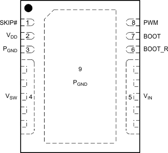 Figure 1. Top View
Pin Description
| PIN | DESCRIPTION | |
|---|---|---|
| NO. | NAME | |
| 1 | SKIP# | This pin enables the Diode Emulation function. When this pin is held Low, Diode Emulation Mode is enabled for the Sync FET. When SKIP# is High, the CSD95375Q4M operates in Forced Continuous Conduction Mode. A tri-state voltage on SKIP# puts the driver into a very low power state. |
| 2 | VDD | Supply Voltage to Gate Drivers and internal circuitry. |
| 3 | PGND | Power Ground, Needs to be connected to Pin 9 and PCB |
| 4 | VSW | Voltage Switching Node – pin connection to the output inductor. |
| 5 | VIN | Input Voltage Pin. Connect input capacitors close to this pin. |
| 6 | BOOT_R | Bootstrap capacitor connection. Connect a minimum 0.1 µF 16 V X5R, ceramic cap from BOOT to BOOT_R pins. The bootstrap capacitor provides the charge to turn on the Control FET. The bootstrap diode is integrated. Boot_R is internally connected to VSW. |
| 7 | BOOT | |
| 8 | PWM | Pulse Width modulated tri-state input from external controller. Logic Low sets Control FET gate low and Sync FET gate high. Logic High sets Control FET gate high and Sync FET gate Low. Open or High Z sets both MOSFET gates low if greater than the Tri-State Shutdown Hold-off Time (t3HT) |
| 9 | PGND | Power Ground |