SLPS751 January   2023 CSD95411

PRODUCTION DATA  

  1. 1Features
  2. 2Applications
  3. 3Description
  4. 4Revision History
  5. 5Device and Documentation Support
    1. 5.1 Device Support
      1. 5.1.1 Third-Party Products Disclaimer
    2. 5.2 Documentation Support
    3. 5.3 Receiving Notification of Documentation Updates
    4. 5.4 Support Resources
    5. 5.5 Trademarks
    6. 5.6 Electrostatic Discharge Caution
    7. 5.7 Glossary
  6. 6Mechanical, Packaging, and Orderable Information
    1. 6.1 Package Option Addendum
    2. 6.2 Tape and Reel Information
    3. 6.3 Mechanical Drawing
    4. 6.4 Recommended PCB Land Pattern
    5. 6.5 Recommended Stencil Opening
    6. 6.6 Alternate Industry Standard Compatible PCB Land Pattern
    7. 6.7 Alternate Industry Standard Compatible Stencil Opening

Package Options

Mechanical Data (Package|Pins)
  • RRB|41
Thermal pad, mechanical data (Package|Pins)

Recommended PCB Land Pattern

GUID-0A96946C-F0ED-48B1-9639-75BDDD905CFF-low.png

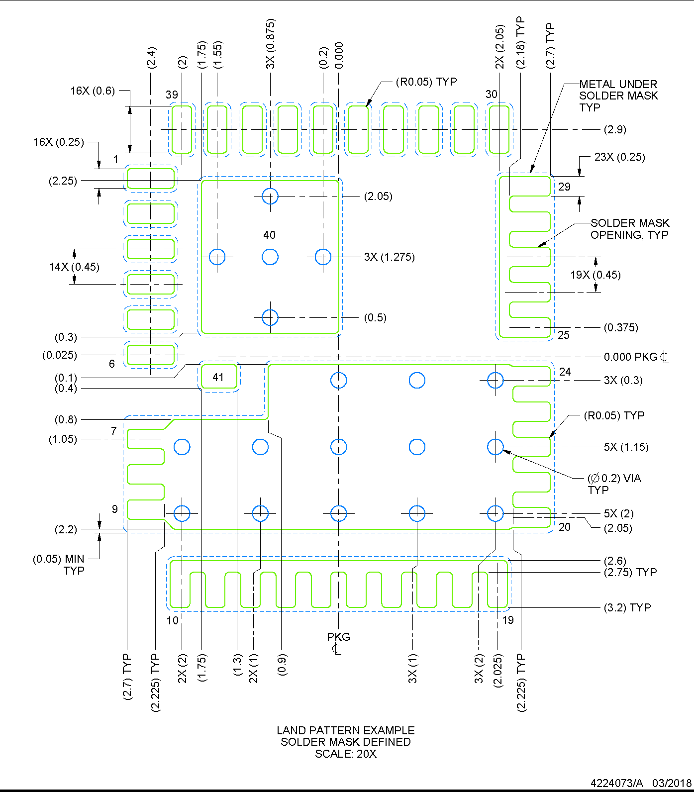
1. All linear dimensions are in millimeters. Any dimensions in parenthesis are for reference only. Dimensioning and tolerancing per ASME Y14.5M.

2. This drawing is subject to change without notice.

3. This package is designed to be soldered to thermal pads on the board. For more information, see QFN/SON PCB Attachment (SLUA271).