SBAS442D august 2008 – august 2023 DAC5311 , DAC6311 , DAC7311
PRODUCTION DATA
- 1
- 1 Features
- 2 Applications
- 3 Description
- 4 Revision History
- 5 Device Comparison
- 6 Pin Configuration and Functions
-
7 Specifications
- 7.1 Absolute Maximum Ratings
- 7.2 ESD Ratings
- 7.3 Recommended Operating Conditions
- 7.4 Thermal Information
- 7.5 Electrical Characteristics
- 7.6 Timing Requirements
- 7.7 Timing Diagrams
- 7.8 Typical Characteristics: AVDD = 5 V
- 7.9 Typical Characteristics: AVDD = 3.6 V
- 7.10 Typical Characteristics: AVDD = 2.7 V
- 8 Detailed Description
- 9 Application and Implementation
- 10Device and Documentation Support
- 11Mechanical, Packaging, and Orderable Information
Package Options
Mechanical Data (Package|Pins)
- DCK|6
Thermal pad, mechanical data (Package|Pins)
- DCK|6
Orderable Information
9.2.2 Using the REF5050 as a Power Supply for the DACx311
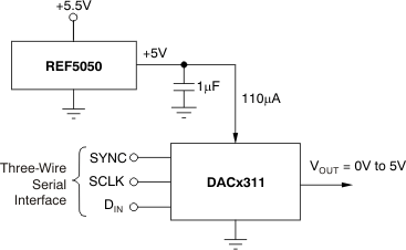
As a result of the extremely low supply current required by the DACx311, an alternative option is to use a REF5050 5-V precision voltage reference to supply the required voltage to the part, as shown in Figure 9-8. This option is especially useful if the power supply is too noisy or if the system supply voltages are at some value other than 5 V. The REF5050 outputs a steady supply voltage for the DACx311. If the REF5050 is used, the current needed to supply DACx311 is typically 110 μA at 5 V, with no load on the output of the DAC. When the DAC output is loaded, the REF5050 also needs to supply the current to the load. The total current required (with a 5 kΩ load on the DAC output) is:
The load regulation of the REF5050 is typically 0.002%/mA, which results in an error of 90 μV for the 1.1 mA current drawn from the device. This value corresponds to a 0.07 LSB error at 12 bits (DAC7311).
 Figure 9-8 REF5050 as Power Supply to DACx311
For other power-supply voltages, alternative references such as the REF3030 (3 V), REF3033 (3.3 V), or REF3220 (2.048 V) are recommended. For a full list of available voltage references from TI, see the TI web site at www.ti.com.