SLASER3A July   2018  – November 2018 DAC61408 , DAC71408 , DAC81408

PRODUCTION DATA.  

  1. Features
  2. Applications
  3. Description
    1.     Device Images
      1.      Functional Block Diagram
  4. Revision History
  5. Device Comparison Table
  6. Pin Configuration and Functions
    1.     Pin Functions
  7. Specifications
    1. 7.1 Absolute Maximum Ratings
    2. 7.2 ESD Ratings
    3. 7.3 Recommended Operating Conditions
    4. 7.4 Thermal Information
    5. 7.5 Electrical Characteristics
    6. 7.6 Timing Requirements
    7. 7.7 Typical Characteristics
  8. Parameter Measurement Information
  9. Detailed Description
    1. 9.1 Overview
    2. 9.2 Functional Block Diagram
    3. 9.3 Feature Description
      1. 9.3.1 Digital-to-Analog Converters (DACs) Architecture
        1. 9.3.1.1 DAC Transfer Function
        2. 9.3.1.2 DAC Register Structure
          1. 9.3.1.2.1 DAC Register Synchronous and Asynchronous Updates
          2. 9.3.1.2.2 Broadcast DAC Register
          3. 9.3.1.2.3 Clear DAC Operation
      2. 9.3.2 Internal Reference
      3. 9.3.3 Device Reset Options
        1. 9.3.3.1 Power-on-Reset (POR)
        2. 9.3.3.2 Hardware Reset
        3. 9.3.3.3 Software Reset
      4. 9.3.4 Thermal Protection
        1. 9.3.4.1 Analog Temperature Sensor: TEMPOUT Pin
        2. 9.3.4.2 Thermal Shutdown
    4. 9.4 Device Functional Modes
      1. 9.4.1 Toggle Mode
      2. 9.4.2 Differential Mode
      3. 9.4.3 Power-Down Mode
    5. 9.5 Programming
      1. 9.5.1 Stand-Alone Operation
        1. 9.5.1.1 Streaming Mode Operation
      2. 9.5.2 Daisy-Chain Operation
      3. 9.5.3 Frame Error Checking
    6. 9.6 Register Maps
      1. 9.6.1  NOP Register (Offset = 00h) [reset = 0000h]
        1. Table 9. NOP Register Field Descriptions
      2. 9.6.2  DEVICEID Register (Offset = 01h) [reset = ----h]
        1. Table 10. DEVICEID Register Field Descriptions
      3. 9.6.3  STATUS Register (Offset = 02h) [reset = 0000h]
        1. Table 11. STATUS Register Field Descriptions
      4. 9.6.4  SPICONFIG Register (Offset = 03h) [reset = 0A24h]
        1. Table 12. SPICONFIG Register Field Descriptions
      5. 9.6.5  GENCONFIG Register (Offset = 04h) [reset = 7F00h]
        1. Table 13. GENCONFIG Register Field Descriptions
      6. 9.6.6  BRDCONFIG Register (Offset = 05h) [reset = FFFFh]
        1. Table 14. BRDCONFIG Register Field Descriptions
      7. 9.6.7  SYNCCONFIG Register (Offset = 06h) [reset = 0000h]
        1. Table 15. SYNCCONFIG Register Field Descriptions
      8. 9.6.8  TOGGCONFIG0 Register (Offset = 07h) [reset = 0000h]
        1. Table 16. TOGGCONFIG0 Register Field Descriptions
      9. 9.6.9  TOGGCONFIG1 Register (Offset = 08h) [reset = 0000h]
        1. Table 17. TOGGCONFIG1 Register Field Descriptions
      10. 9.6.10 DACPWDWN Register (Offset = 09h) [reset = FFFFh]
        1. Table 18. DACPWDWN Register Field Descriptions
      11. 9.6.11 DACRANGEn Register (Offset = 0Bh - 0Ch) [reset = 0000h]
        1. Table 19. DACRANGEn Register Field Descriptions
      12. 9.6.12 TRIGGER Register (Offset = 0Eh) [reset = 0000h]
        1. Table 20. TRIGGER Register Field Descriptions
      13. 9.6.13 BRDCAST Register (Offset = 0Fh) [reset = 0000h]
        1. Table 21. BRDCAST Register Field Descriptions
      14. 9.6.14 DACn Register (Offset = 14h - 1Bh) [reset = 0000h]
        1. Table 22. DACn Register Field Descriptions
      15. 9.6.15 OFFSETn Register (Offset = 21h - 22h) [reset = 0000h]
        1. Table 23. OFFSETn Register Field Descriptions
  10. 10Application and Implementation
    1. 10.1 Application Information
    2. 10.2 Typical Application
      1. 10.2.1 Design Requirements
      2. 10.2.2 Detailed Design Procedure for Remote Ground Tracking
        1. 10.2.2.1 Generating 300mV Offset
        2. 10.2.2.2 Amplifier Selection
        3. 10.2.2.3 Passive Component Selection
      3. 10.2.3 Application Curves
  11. 11Power Supply Recommendations
  12. 12Layout
    1. 12.1 Layout Guidelines
    2. 12.2 Layout Example
  13. 13Device and Documentation Support
    1. 13.1 Documentation Support
    2. 13.2 Related Links
    3. 13.3 Receiving Notification of Documentation Updates
    4. 13.4 Community Resources
    5. 13.5 Trademarks
    6. 13.6 Electrostatic Discharge Caution
    7. 13.7 Glossary
  14. 14Mechanical, Packaging, and Orderable Information

Package Options

Refer to the PDF data sheet for device specific package drawings

Mechanical Data (Package|Pins)
  • RHA|40
Thermal pad, mechanical data (Package|Pins)
Orderable Information

Typical Characteristics

at TA = 25°C, VDD = VAA = 5 V, VREFIN = 2.5 V. Unipolar ranges: VSS = 0 V and VCC ≥ VMAX + 1.5 V for the DAC range. Bipolar ranges: VSS ≤ VMIN – 1.5 V and VCC ≥ VMAX + 1.5 V for the DAC range. DAC outputs unloaded, unless otherwise noted.
DAC81408 DAC71408 DAC61408 D001_SLASER3.gif
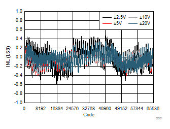
Figure 1. Integral Linearity Error vs Digital Input Code (Bipolar Outputs)
DAC81408 DAC71408 DAC61408 D003_SLASER3.gif
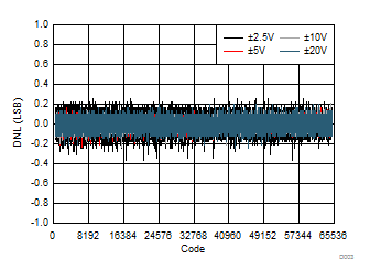
Figure 3. Differential Linearity Error vs Digital Input Code (Bipolar Outputs)
DAC81408 DAC71408 DAC61408 D005_SLASER3.gif
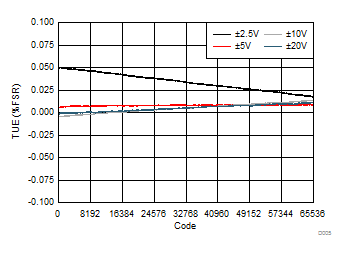
Figure 5. Total Unadjusted Error vs Digital Input Code (Bipolar Outputs)
DAC81408 DAC71408 DAC61408 D007_SLASER3.gif
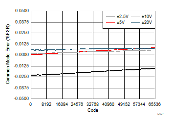
Figure 7. Common Mode Error vs Digital Input Code (Differential Bipolar Outputs)
DAC81408 DAC71408 DAC61408 D009_SLASER3.gif
±20-V Output Range
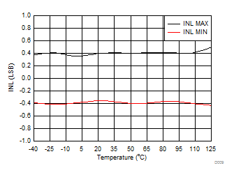
Figure 9. Integral Linearity Error vs Temperature
DAC81408 DAC71408 DAC61408 D011_SLASER3.gif
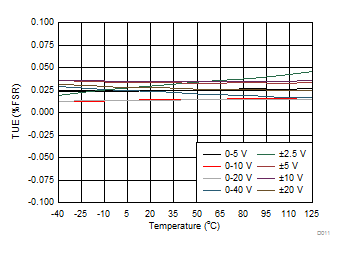
Figure 11. Total Unadjusted Error vs Temperature
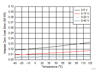
DAC81408 DAC71408 DAC61408 D013_SLASER3.gif
Figure 13. Unipolar Zero Code Error vs Temperature
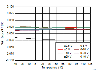
DAC81408 DAC71408 DAC61408 D015_SLASER3.gif
Figure 15. Gain Error vs Temperature
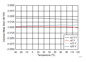
DAC81408 DAC71408 DAC61408 D017_SLASER3.gif
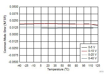
Figure 17. Common Mode Error vs Temperature (Differential Bipolar Outputs)
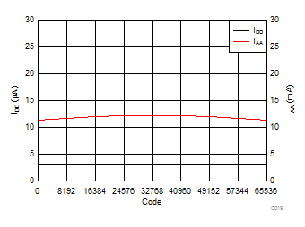
DAC81408 DAC71408 DAC61408 D019_SLASER3.gif
±20-V Output Range
Figure 19. Supply Current (IDD, IAA) vs Digital Input Code
DAC81408 DAC71408 DAC61408 D021_SLASER3.gif
±20-V Output Range
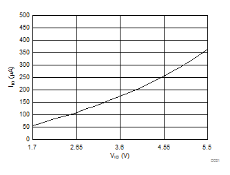
Figure 21. Supply Current (IIO) vs Supply Voltage
DAC81408 DAC71408 DAC61408 D023_SLASER3.gif
±20-V Output Range
Figure 23. Power-Down Current vs Temperature
DAC81408 DAC71408 DAC61408 D025_SLASER3.gif
Full-scale Code
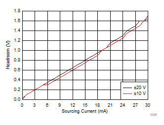
Figure 25. VCC Headroom vs Sourcing Current
DAC81408 DAC71408 DAC61408 D027_SLASER3.gif
±20-V Output Range
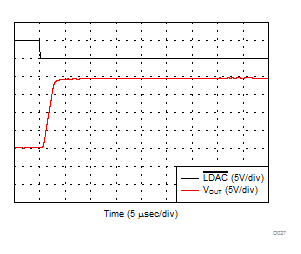
Figure 27. Full-Scale Settling Time, Rising Edge
DAC81408 DAC71408 DAC61408 D029_SLASER3.gif
Power-down to Active DAC Mode
±20-V Output Range
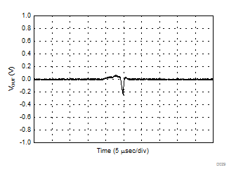
Figure 29. DAC Output Enable Glitch
DAC81408 DAC71408 DAC61408 D031_SLASER3.gif
±20-V Output Range
Toggle signal: 1 VPP
DC Change: Midscale to 3/4 Full-scale
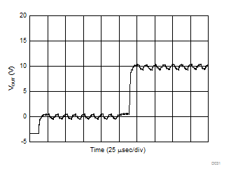
Figure 31. Toggle Output Change Response
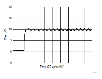
DAC81408 DAC71408 DAC61408 D033_SLASER3.gif
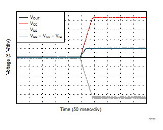
Figure 33. Power-Up Response
DAC81408 DAC71408 DAC61408 D035_SLASER3.gif
±20-V Output Range
Full-scale Code to 0 V
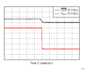
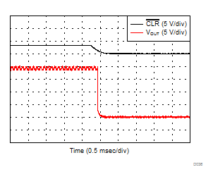
Figure 35. Clear Command Response
DAC81408 DAC71408 DAC61408 D037_SLASER3.gif
0 to 5-V Output Range
Midscale Code
Figure 37. DAC Output Noise Density vs Frequency
DAC81408 DAC71408 DAC61408 D039_SLASER3.gif
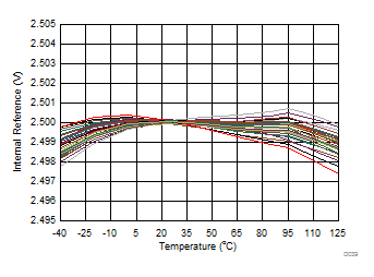
Figure 39. Internal Reference Voltage vs Temperature
DAC81408 DAC71408 DAC61408 D041_SLASER3.gif
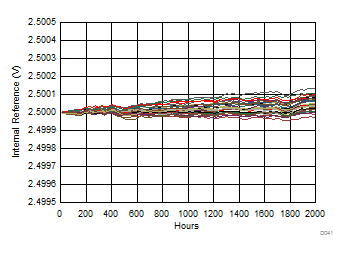
Figure 41. Internal Reference Voltage vs Time
DAC81408 DAC71408 DAC61408 D043_SLASER3.gif
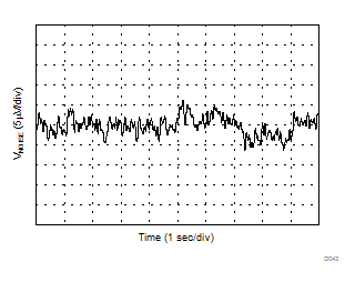
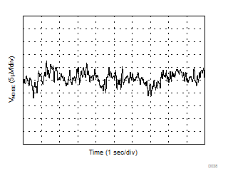
Figure 43. Internal Reference Noise
DAC81408 DAC71408 DAC61408 D002_SLASER3.gif
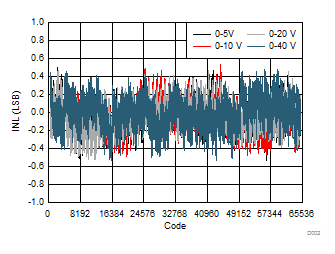
Figure 2. Integral Linearity Error vs Digital Input Code (Unipolar Outputs)
DAC81408 DAC71408 DAC61408 D004_SLASER3.gif
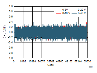
Figure 4. Differential Linearity Error vs Digital Input Code (Unipolar Outputs)
DAC81408 DAC71408 DAC61408 D006_SLASER3.gif
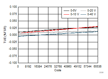
Figure 6. Total Unadjusted Error vs Digital Input Code (Unipolar Outputs)
DAC81408 DAC71408 DAC61408 D008_SLASER3.gif
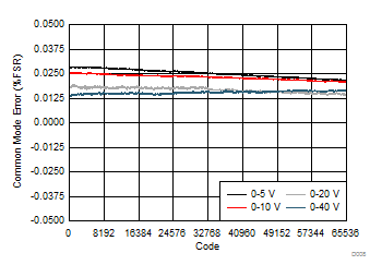
Figure 8. Common Mode Error vs Digital Input Code (Differential Unipolar Outputs)
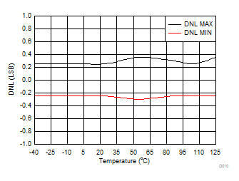
DAC81408 DAC71408 DAC61408 D010_SLASER3.gif
±20-V Output Range
Figure 10. Differential Linearity Error vs Temperature
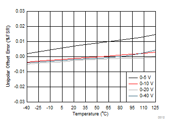
DAC81408 DAC71408 DAC61408 D012_SLASER3.gif
Figure 12. Unipolar Offset Error vs Temperature
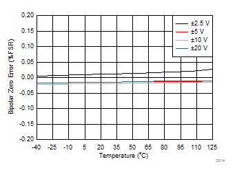
DAC81408 DAC71408 DAC61408 D014_SLASER3.gif
Figure 14. Bipolar Zero Error vs Temperature
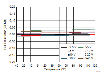
DAC81408 DAC71408 DAC61408 D016_SLASER3.gif
Figure 16. Full-Scale Error vs Temperature
DAC81408 DAC71408 DAC61408 D018_SLASER3.gif
Figure 18. Common Mode Error vs Temperature (Differential Unipolar Outputs)
DAC81408 DAC71408 DAC61408 D020_SLASER3.gif
±20-V Output Range
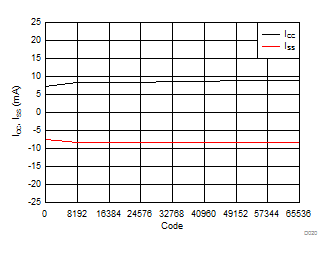
Figure 20. Supply Current (ICC, ISS) vs Digital Input Code
DAC81408 DAC71408 DAC61408 D022_SLASER3.gif
±20-V Output Range
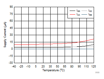
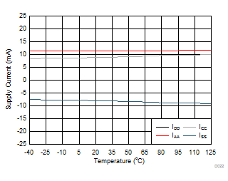
Figure 22. Supply Current vs Temperature
DAC81408 DAC71408 DAC61408 D024_SLASER3.gif
±20-V Output Range
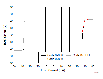
Figure 24. Source and Sink Capability
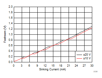
DAC81408 DAC71408 DAC61408 D026_SLASER3.gif
Zero Code
Figure 26. VSS Footroom vs Sinking Current
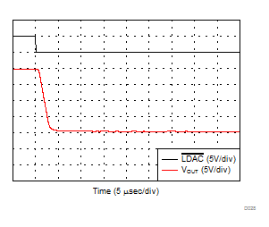
DAC81408 DAC71408 DAC61408 D028_SLASER3.gif
±20-V Output Range
Figure 28. Full-Scale Settling Time, Falling Edge
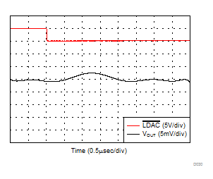
DAC81408 DAC71408 DAC61408 D030_SLASER3.gif
0 to 5-V Output Range
Figure 30. Glitch Impulse, 1 LSB Step
DAC81408 DAC71408 DAC61408 D032_SLASER3.gif
±20-V Output Range
Toggle signal: 1 VPP
DC value: 3/4 Full-scale
Figure 32. Toggle Enable Response
DAC81408 DAC71408 DAC61408 D034_SLASER3.gif
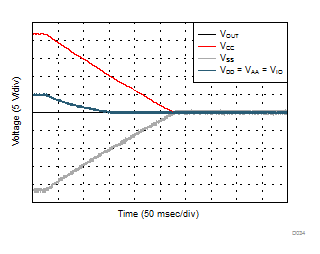
Figure 34. Power-Down Response
DAC81408 DAC71408 DAC61408 D036_SLASER3.gif
±20-V Output Range
Toggle signal: 1 VPP
DC value at 20 V
Figure 36. Clear Command Response in Toggle Mode
DAC81408 DAC71408 DAC61408 D038_SLASER3.gif
0 to 5-V Output Range
Midscale Code
Figure 38. DAC Output Noise
DAC81408 DAC71408 DAC61408 D040_SLASER3.gif
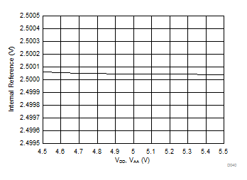
Figure 40. Internal Reference Voltage vs Supply Voltage
DAC81408 DAC71408 DAC61408 D042_SLASER3.gif
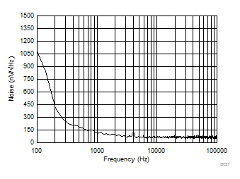
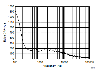
Figure 42. Internal Reference Noise Density vs Frequency
DAC81408 DAC71408 DAC61408 D044_SLASER3.gif
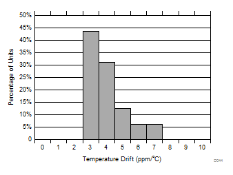
Figure 44. Internal Reference Temperature Drift Histogram