SBAS430F January 2009 – April 2018 DAC7568 , DAC8168 , DAC8568
PRODUCTION DATA.
- 1 Features
- 2 Applications
- 3 Description
- 4 Revision History
- 5 Device Comparison Table
- 6 Pin Configuration and Functions
- 7 Specifications
-
8 Detailed Description
- 8.1 Functional Block Diagram
- 8.2
Feature Description
- 8.2.1 Digital-to-Analog Converter (DAC)
- 8.2.2 Resistor String
- 8.2.3 Output Amplifier
- 8.2.4 Internal Reference
- 8.2.5 Serial Interface
- 8.2.6 Input Shift Register
- 8.2.7 SYNC Interrupt
- 8.2.8 Power-on Reset to Zero Scale or Midscale
- 8.2.9 Clear Code Register and CLR Pin
- 8.2.10 Software Reset Function
- 8.2.11
Operating Examples: DAC7568/DAC8168/DAC8568
- Table 4. 1st: Write to Data Buffer A:
- Table 5. 2nd: Write to Data Buffer B:
- Table 6. 3rd: Write to Data Buffer G:
- Table 7. 4th: Write to Data Buffer H and Simultaneously Update all DACs:
- Table 8. 1st: Write to Data Buffer C and Load DAC C: DAC C Output Settles to Specified Value Upon Completion:
- Table 9. 2nd: Write to Data Buffer D and Load DAC D: DAC D Output Settles to Specified Value Upon Completion:
- Table 10. 3rd: Write to Data Buffer E and Load DAC E: DAC E Output Settles to Specified Value Upon Completion:
- Table 11. 4th: Write to Data Buffer F and Load DAC F: DAC F Output Settles to Specified Value Upon Completion:
- Table 12. 1st: Write Power-Down Command to DAC Channel A and DAC Channel B: DAC A and DAC B to 1kΩ.
- Table 13. 2nd: Write Power-Down Command to DAC Channel H: DAC H to 1kΩ.
- Table 14. 3rd: Write Power-Down Command to DAC Channel C and DAC Channel D: DAC C and DAC D to 100kΩ.
- Table 15. 4th: Write Power-Down Command to DAC Channel F: DAC F to 100kΩ.
- Table 16. 1st: Write Sequence for Enabling the DAC7568, DAC8168, and DAC8568 Internal Reference All the Time:
- Table 17. 2nd: Write Sequence to Power-Down All DACs to High-Impedance:
- Table 18. 1st: Write Sequence for Disabling the DAC7568, DAC8168, and DAC8568 Internal Reference All the Time (after this sequence, these devices require an external reference source to function):
- Table 19. 2nd: Write Sequence to Write Specified Data to All DACs:
- 8.3
Device Functional Modes
- 8.3.1
Enable/Disable Internal Reference
- 8.3.1.1 Static Mode
- 8.3.1.2
Flexible Mode
- Table 22. Write Sequence for Enabling Internal Reference (Flexible Mode) (Internal Reference Powered On—09080000h)
- Table 23. Write Sequence for Enabling Internal Reference (Flexible Mode) (Internal Reference Always Powered On—090A0000h)
- Table 24. Write Sequence for Disabling Internal Reference (Flexible Mode) (Internal Reference Always Powered Down—090C0000h)
- Table 25. Write Sequence for Switching from Flexible Mode to Static Mode for Internal Reference (Internal Reference Always Powered Down—09000000h)
- 8.3.2 LDAC Functionality
- 8.3.3 Power-Down Modes
- 8.3.1
Enable/Disable Internal Reference
-
9 Application and Implementation
- 9.1 Application Information
- 9.2
Typical Applications - Microprocessor Interfacing
- 9.2.1 DAC7568/DAC8168/DAC8568 to an 8051 Interface
- 9.2.2 DAC7568/DAC8168/DAC8568 to Microwire Interface
- 9.2.3 DAC7568/DAC8168/DAC8568 to 68HC11 Interface
- 10Layout
-
11Device and Documentation Support
- 11.1
Device Support
- 11.1.1
Device Nomenclature
- 11.1.1.1
Static Performance
- 11.1.1.1.1 Resolution
- 11.1.1.1.2 Least Significant Bit (LSB)
- 11.1.1.1.3 Most Significant Bit (MSB)
- 11.1.1.1.4 Relative Accuracy or Integral Nonlinearity (INL)
- 11.1.1.1.5 Differential Nonlinearity (DNL)
- 11.1.1.1.6 Full-Scale Error
- 11.1.1.1.7 Offset Error
- 11.1.1.1.8 Zero-Code Error
- 11.1.1.1.9 Gain Error
- 11.1.1.1.10 Full-Scale Error Drift
- 11.1.1.1.11 Offset Error Drift
- 11.1.1.1.12 Zero-Code Error Drift
- 11.1.1.1.13 Gain Temperature Coefficient
- 11.1.1.1.14 Power-Supply Rejection Ratio (PSRR)
- 11.1.1.1.15 Monotonicity
- 11.1.1.2
Dynamic Performance
- 11.1.1.2.1 Slew Rate
- 11.1.1.2.2 Output Voltage Settling Time
- 11.1.1.2.3 Code Change/Digital-to-Analog Glitch Energy
- 11.1.1.2.4 Digital Feedthrough
- 11.1.1.2.5 Channel-to-Channel DC Crosstalk
- 11.1.1.2.6 Channel-to-Channel AC Crosstalk
- 11.1.1.2.7 Signal-to-Noise Ratio (SNR)
- 11.1.1.2.8 Total Harmonic Distortion (THD)
- 11.1.1.2.9 Spurious-Free Dynamic Range (SFDR)
- 11.1.1.2.10 Signal-to-Noise plus Distortion (SINAD)
- 11.1.1.2.11 DAC Output Noise Density
- 11.1.1.2.12 DAC Output Noise
- 11.1.1.2.13 Full-Scale Range (FSR)
- 11.1.1.1
Static Performance
- 11.1.1
Device Nomenclature
- 11.2 Related Links
- 11.3 Receiving Notification of Documentation Updates
- 11.4 Community Resources
- 11.5 Trademarks
- 11.6 Electrostatic Discharge Caution
- 11.7 Glossary
- 11.1
Device Support
- 12Mechanical, Packaging, and Orderable Information
Package Options
Mechanical Data (Package|Pins)
Thermal pad, mechanical data (Package|Pins)
Orderable Information
7.5 Typical Characteristics: DAC at AVDD = 5.5 V
Channel-specific information provided as examples. At TA = +25°C, external reference used, DAC output not loaded, and all DAC codes in straight binary data format, unless otherwise noted.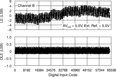 Figure 14. Linearity Error and Differential Linearity Error vs Digital Input Code (–40°C)
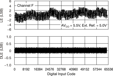 Figure 16. Linearity Error and Differential Linearity Error vs Digital Input Code (–40°C)
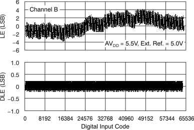 Figure 18. Linearity Error and Differential Linearity Error vs Digital Input Code (+25°C)
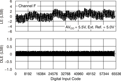 Figure 20. Linearity Error and Differential Linearity Error vs Digital Input Code (+25°C)
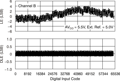 Figure 22. Linearity Error and Differential Linearity Error vs Digital Input Code (+125°C)
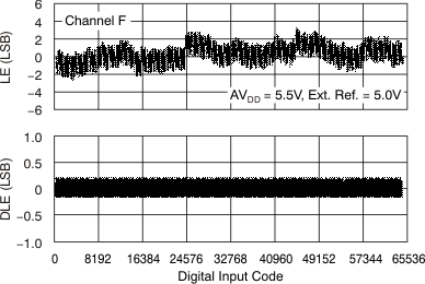 Figure 24. Linearity Error and Differential Linearity Error vs Digital Input Code (+125°C)
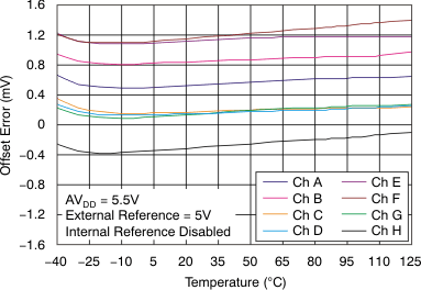 Figure 26. Offset Error vs Temperature
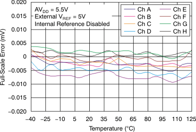 Figure 28. Full-Scale Error vs Temperature
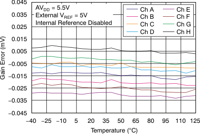 Figure 30. Gain Error vs Temperature
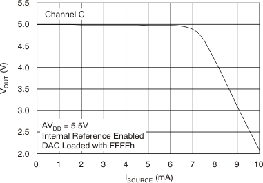 Figure 32. Source Current at Positive Rail (Grades C and D)
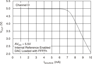 Figure 34. Source Current at Positive Rail (Grades C and D)
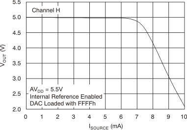 Figure 36. Source Current at Positive Rail (Grades C and D)
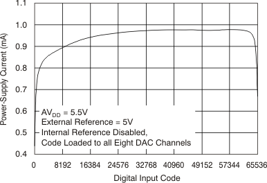 Figure 38. Power-Supply Current vs Digital Input Code
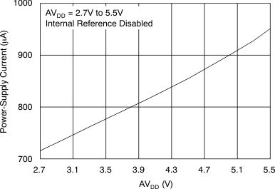 Figure 40. Power-Supply Current vs Power-Supply Voltage
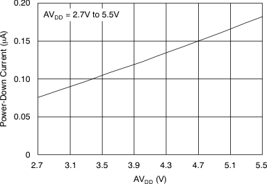 Figure 42. Power-Down Current vs Power-Supply Voltage
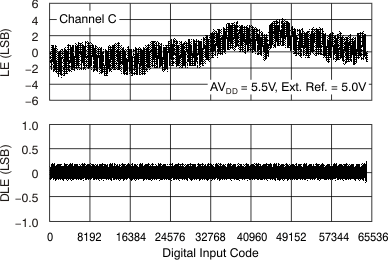 Figure 15. Linearity Error and Differential Linearity Error vs Digital Input Code (–40°C)
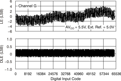 Figure 17. Linearity Error and Differential Linearity Error vs Digital Input Code (–40°C)
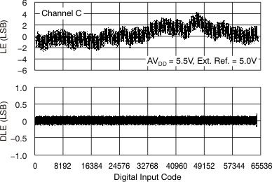 Figure 19. Linearity Error and Differential Linearity Error vs Digital Input Code (+25°C)
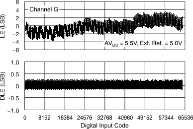 Figure 21. Linearity Error and Differential Linearity Error vs Digital Input Code (+25°C)
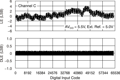 Figure 23. Linearity Error and Differential Linearity Error vs Digital Input Code (+125°C)
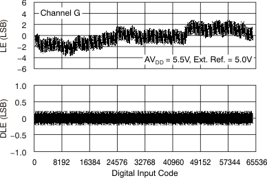 Figure 25. Linearity Error and Differential Linearity Error vs Digital Input Code (+125°C)
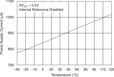 Figure 27. Power-Supply Current vs Temperature
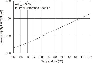 Figure 29. Power-Supply Current vs Temperature
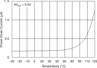 Figure 31. Power-Down Current vs Temperature
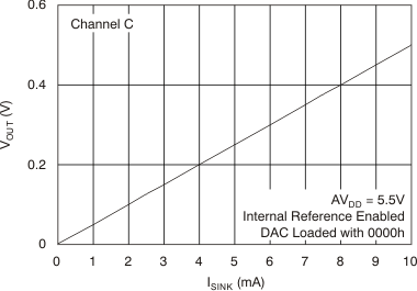 Figure 33. Sink Current at Negative Rail (All Grades)
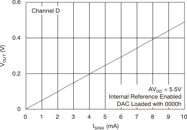 Figure 35. Sink Current at Negative Rail (All Grades)
 Figure 37. Sink Current at Negative Rail (All Grades)
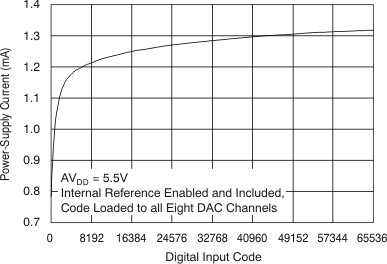 Figure 39. Power-Supply Current vs Digital Input Code
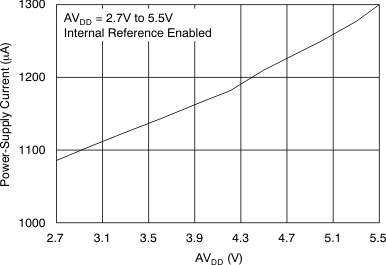 Figure 41. Power-Supply Current vs Power-Supply Voltage
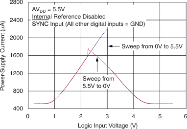 Figure 43. Power-Supply Current vs Logic Input Voltage
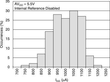 Figure 45. Power-Supply Current Histogram
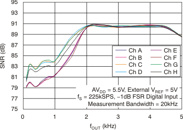 Figure 47. Signal-to-Noise Ratio vs Output Frequency
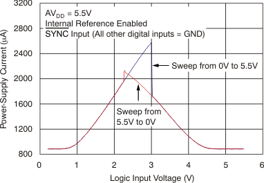 Figure 44. Power-Supply Current vs Logic Input Voltage
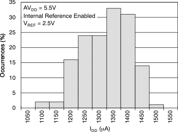 Figure 46. Power-Supply Current Histogram
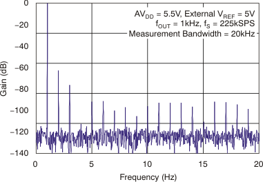 Figure 48. Power Spectral Density
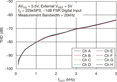 Figure 50. Third Harmonic Distortion vs Output Frequency
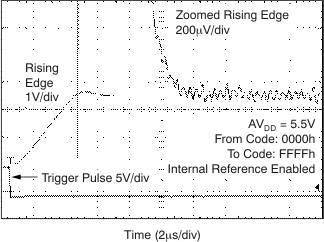 Figure 52. Full-Scale Settling Time: 5-V Rising Edge
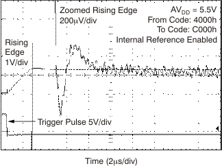 Figure 54. Half-Scale Settling Time: 5-V Rising Edge
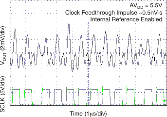 Figure 56. Clock Feedthrough 2 Mhz, Midscale
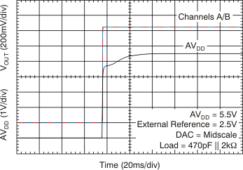 Figure 58. Power-On Glitch Reset To Midscale
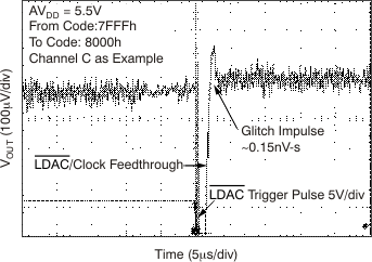 Figure 60. Glitch Energy: 5 V, 1-LSB Step, Rising Edge
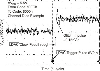 Figure 62. Glitch Energy: 5 V, 4-LSB Step, Rising Edge
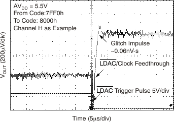 Figure 64. Glitch Energy: 5 V, 16-LSB Step, Rising Edge
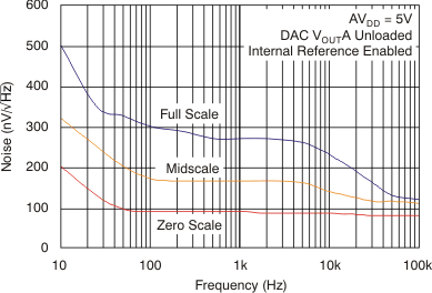
| See the Application Information section of this data sheet for more details. |
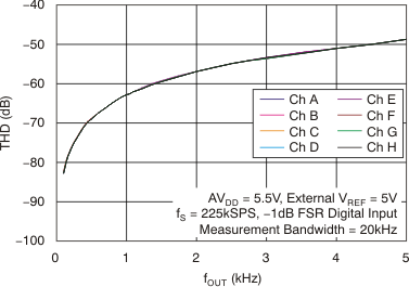 Figure 49. Second Harmonic Distortion vs Output Frequency
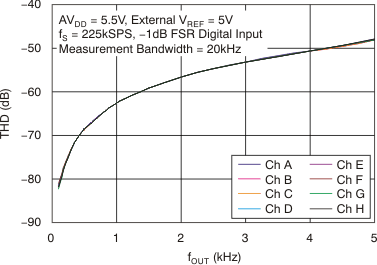 Figure 51. Total Harmonic Distortion vs Output Frequency
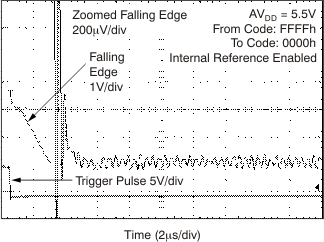 Figure 53. Full-Scale Settling Time: 5-V Falling Edge
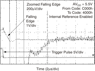 Figure 55. Half-Scale Settling Time: 5-V Falling Edge
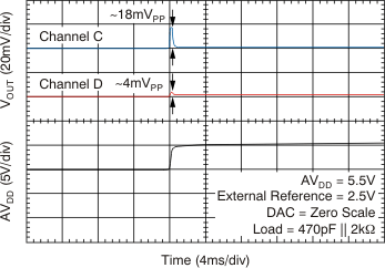 Figure 57. Power-On Glitch Reset to Zero Scale
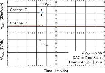 Figure 59. Power-Off Glitch
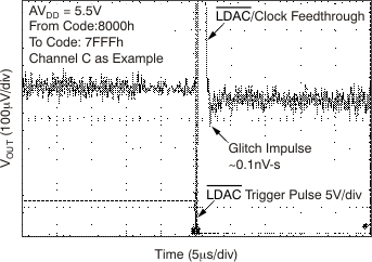 Figure 61. Glitch Energy: 5 V, 1-LSB Step, Falling Edge
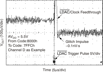 Figure 63. Glitch Energy: 5 V, 4-LSB Step, Falling Edge
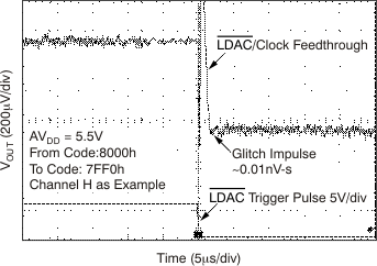 Figure 65. Glitch Energy: 5 V, 16-LSB Step, Falling Edge
