SBVS011N March 2000 – April 2020 DCP020503 , DCP020505 , DCP020507 , DCP020509 , DCP020515D , DCP021205 , DCP021212 , DCP021212D , DCP021515 , DCP022405 , DCP022405D , DCP022415D
PRODUCTION DATA
- 1Features
- 2Applications
- 3Description
- 4Revision History
- 5Pin Configuration and Functions
- 6Specifications
-
7Detailed Description
- 7.1 Overview
- 7.2 Functional Block Diagrams
- 7.3 Feature Description
- 7.4 Device Functional Modes
- 8Layout
- 9Device and Documentation Support
Package Options
Mechanical Data (Package|Pins)
Thermal pad, mechanical data (Package|Pins)
Orderable Information
3 Description
The DCP02 series is a family of 2-W, isolated, unregulated DC/DC converter modules. Requiring a minimum of external components and including on-chip device protection, the DCP02 series of devices provide extra features such as output disable and synchronization of switching frequencies.
This combination of features and small size makes the DCP02 series of devices suitable for a wide range of applications, and is an easy-to-use solution in applications requiring signal path isolation.
WARNING: This product has
operational isolation and is intended for signal isolation only. It should not be
used as a part of a safety isolation circuit requiring reinforced isolation. See
definitions in Feature Description
Device
Information
| PART NUMBER | PACKAGE(1) | BODY SIZE (NOM) |
|---|---|---|
| DCP02xxxx | PDIP (7) | 19.18 mm × 10.60 mm |
| SOP (12) | 17.90 mm × 10.33 mm |
(1) For all available packages, see the orderable addendum at the end of the data sheet.
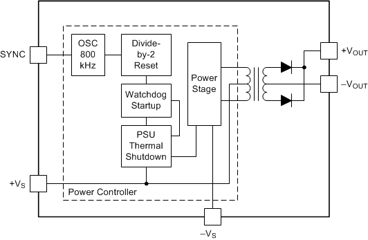
 Single Output Block
Diagram
 Dual Output Block
Diagram