SBAS368D May 2006 – December 2016 DDC264
PRODUCTION DATA.
- 1 Features
- 2 Applications
- 3 Description
- 4 Revision History
- 5 Device Comparison Table
- 6 Pin Configuration and Functions
- 7 Specifications
-
8 Detailed Description
- 8.1 Overview
- 8.2 Functional Block Diagram
- 8.3
Feature Description
- 8.3.1 Dual Switched Integrator: Basic Integration Cycle
- 8.3.2 Integration Capacitors
- 8.3.3 Voltage Reference
- 8.3.4 Serial Data Output and Control Interface
- 8.4 Device Functional Modes
- 8.5 Programming
- 8.6 Register Maps
- 9 Application and Implementation
- 10Power Supply Recommendations
- 11Layout
- 12Device and Documentation Support
- 13Mechanical, Packaging, and Orderable Information
Package Options
Mechanical Data (Package|Pins)
- ZAW|100
Thermal pad, mechanical data (Package|Pins)
Orderable Information
10 Power Supply Recommendations
10.1 Power-Up Sequencing
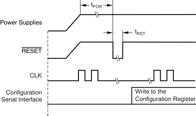
Before device power-up, all digital and analog inputs must be low. At the time of power-up, all of these signals must remain low until the power supplies have stabilized, as shown in Figure 34. The analog supply must come up before or at the same time as the digital supply. At this time, begin supplying the master clock signal to the CLK pin. Wait for time tPOR, then give a RESET pulse. After releasing RESET, the Configuration Register must be written. Table 11 shows the timing for the power-up sequence.
 Figure 34. DDC264 Timing Diagram at Power-Up
Table 11. Timing for DDC264 Power-Up Sequence
| MIN | TYP | MAX | UNIT | ||
|---|---|---|---|---|---|
| tPOR | Wait after power-up until reset | 250 | ms | ||
10.2 Power Supplies and Grounding
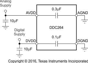
Both AVDD and DVDD must be as quiet as possible. It is particularly important to eliminate noise from AVDD that is non-synchronous with the DDC264 operation. Figure 35 illustrates how to supply power to the DDC264. Each DDC264 has internal bypass capacitors on AVDD and DVDD; therefore, the only external bypass capacitors typically required are 10-µF ceramic capacitors, one per PCB. TI recommends connecting both the analog and digital grounds (AGND and DGND) to a single ground plane on the PCB.
 Figure 35. Power Supply Connections