DLPS159C April 2019 – February 2023 DLP470NE
PRODUCTION DATA
- 1 Features
- 2 Applications
- 3 Description
- 4 Revision History
- 5 Pin Configuration and Functions
-
6 Specifications
- 6.1 Absolute Maximum Ratings
- 6.2 Storage Conditions
- 6.3 ESD Ratings
- 6.4 Recommended Operating Conditions
- 6.5 Thermal Information
- 6.6 Electrical Characteristics
- 6.7 Capacitance at Recommended Operating Conditions
- 6.8 Timing Requirements
- 6.9 System Mounting Interface Loads
- 6.10 Micromirror Array Physical Characteristics
- 6.11 Micromirror Array Optical Characteristics
- 6.12 Window Characteristics
- 6.13 Chipset Component Usage Specification
- 7 Detailed Description
- 8 Application and Implementation
- 9 Power Supply Recommendations
- 10Layout
- 11Device and Documentation Support
Package Options
Mechanical Data (Package|Pins)
- FXH|257
Thermal pad, mechanical data (Package|Pins)
Orderable Information
6.11 Micromirror Array Optical Characteristics
Table 6-3 Micromirror Array Optical
Characteristics
| PARAMETER | MIN | NOM | MAX | UNIT | |
|---|---|---|---|---|---|
| Mirror Tilt angle, variation device to device#DLPS1598709#T5021507-5 #T5021507-6#DLPS1598306 | 15.6 | 17.0 | 18.4 | degrees | |
| Number of out-of-specification micromirrors #T4589833-6 | Adjacent micromirrors | 0 | micromirrors | ||
| Non-Adjacent micromirrors | 10 | ||||
| DMD Efficiency (420 nm – 680 nm) |
68 |
% |
|||
(1) Measured relative to the plane formed by the overall micromirror array
(2) Variation can occur between any two individual
micromirrors
located on the same device or located on different devices
(3) Additional variation exists between the micromirror array and the package
datums. See the package drawing.
(4) See #DLPS1598274.
(5) An out-of-specification micromirror is defined as a micromirror that is unable to transition between the two landed states.

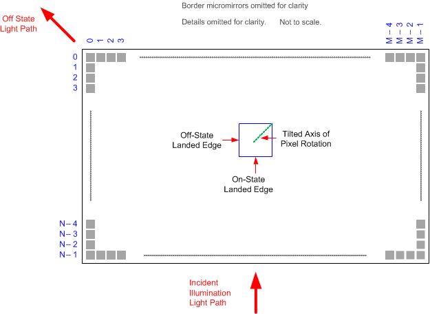
A. Pond of Mirrors (POM) omitted for
clarity
B. Refer to
Micromirror Array Physical Characteristics table
for M, N, and P specifications.
Figure 6-9 Micromirror Landed Orientation and Tilt