DLPS163D April 2019 – December 2023 DLP660TE
PRODUCTION DATA
- 1
- 1 Features
- 2 Applications
- 3 Description
- 4 Pin Configuration and Functions
-
5 Specifications
- 5.1 Absolute Maximum Ratings
- 5.2 Storage Conditions
- 5.3 ESD Ratings
- 5.4 Recommended Operating Conditions
- 5.5 Thermal Information
- 5.6 Electrical Characteristics
- 5.7 Capacitance at Recommended Operating Conditions
- 5.8 Timing Requirements
- 5.9 System Mounting Interface Loads
- 5.10 Micromirror Array Physical Characteristics
- 5.11 Micromirror Array Optical Characteristics
- 5.12 Window Characteristics
- 5.13 Chipset Component Usage Specification
- 6 Detailed Description
- 7 Application and Implementation
- 8 Power Supply Recommendations
- 9 Layout
- 10Device and Documentation Support
- 11Revision History
- 12Mechanical, Packaging, and Orderable Information
Package Options
Mechanical Data (Package|Pins)
- FYG|350
Thermal pad, mechanical data (Package|Pins)
Orderable Information
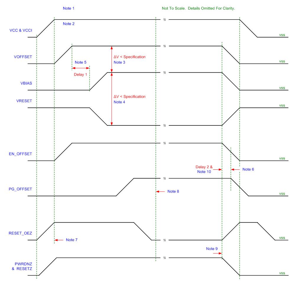
8.2 DMD Power Supply Power-Down Procedure
- During power-down, VCC and VCCI must be supplied until after VBIAS, VRESET, and VOFFSET are discharged to within the specified limit of ground. See Table 8-1.
- During power-down, it is a strict requirement that the voltage delta between VBIAS and VOFFSET must be within the specified limit shown in Section 5.4.
- During power-down, there is no requirement for the relative timing of VRESET with respect to VBIAS.
- Power supply slew rates during power-down are flexible, provided that the transient voltage levels follow the requirements specified in Section 5.1, in Section 5.4, and in Figure 8-1.
- During power-down, LVCMOS input pins must be less than specified in Section 5.4.
 Figure 8-1 DMD Power Supply Requirements
- See Section 4 and Section 5.4.
- To prevent excess current, the supply voltage delta |VCCI – VCC| must be less than specified limit in Section 5.4.
- To prevent excess current, the supply voltage delta |VBIAS – VOFFSET| must be less than specified in Section 5.4.
- To prevent excess current, the supply voltage delta |VBIAS – VRESET| must be less than specified limit in Section 5.4.
- VBIAS must power up after VOFFSET has powered up, per the Delay1 specification in Table 8-1.
- PG_OFFSET must turn off after EN_OFFSET has turned off, per the Delay2 specification in Table 8-1.
- DLP controller software enables the DMD power supplies to turn on after RESET_OEZ is at logic high.
- DLP controller software initiates the global VBIAS command.
- After the DMD micromirror park sequence is complete, the DLP controller software initiates a hardware power-down that activates PWRDNZ and disables VBIAS, VRESET and VOFFSET.
- Under power-loss conditions where emergency DMD micromirror park procedures are being enacted by the DLP controller hardware, EN_OFFSET may turn off after PG_OFFSET has turned off. The OEZ signal goes high prior to PG_OFFSET turning off to indicate the DMD micromirror has completed the emergency park procedures.
Table 8-1 DMD Power-Supply Requirements
| PARAMETER | DESCRIPTION | MIN | NOM | MAX | UNIT |
|---|---|---|---|---|---|
| Delay1 | Delay from VOFFSET settled at recommended operating voltage to VBIAS and VRESET power up | 1 | 2 | ms | |
| Delay2 | PG_OFFSET hold time after EN_OFFSET goes low | 100 | ns |