DLPS047B September 2014 – October 2015 DLPA2005
PRODUCTION DATA.
- 1 Features
- 2 Applications
- 3 Description
- 4 Revision History
- 5 Pin Configuration and Functions
- 6 Specifications
-
7 Detailed Description
- 7.1 Overview
- 7.2 Functional Block Diagram
- 7.3
Feature Description
- 7.3.1 DMD Regulators
- 7.3.2 RGB Strobe Decoder
- 7.3.3 LED Current Control
- 7.3.4 Maximum Led Currents and Efficiency Considerations
- 7.3.5 Calculating Inductor Peak Current
- 7.3.6 LED Current Accuracy
- 7.3.7 Transient Current Limiting
- 7.3.8 1.1-V Regulator (Buck Converter)
- 7.3.9 Measurement System
- 7.3.10
Protection Circuits
- 7.3.10.1 Thermal Warning (HOT) and Thermal Shutdown (TSD)
- 7.3.10.2 Low Battery Warning (BAT_LOW) and Undervoltage Lockout (UVLO)
- 7.3.10.3 DMD Regulator Fault (DMD_FLT)
- 7.3.10.4 V6V Power-Good (V6V_PGF) Fault
- 7.3.10.5 VLED Overvoltage (VLED_OVP) Fault
- 7.3.10.6 VLED Power Save Mode
- 7.3.10.7 V1V8 PG Failure
- 7.3.10.8 Interrupt Pin (INTZ)
- 7.3.10.9 SPI
- 7.3.11 Password Protected Registers
- 7.4 Device Functional Modes
- 7.5 Register Maps
- 8 Application and Implementation
- 9 Power Supply Recommendations
- 10Layout
- 11Device and Documentation Support
- 12Mechanical, Packaging, and Orderable Information
Package Options
Mechanical Data (Package|Pins)
- RSL|48
Thermal pad, mechanical data (Package|Pins)
- RSL|48
Orderable Information
12 Mechanical, Packaging, and Orderable Information
The following pages include mechanical, packaging, and orderable information. This information is the most current data available for the designated devices. This data is subject to change without notice and revision of this document. For browser-based versions of this data sheet, refer to the left-hand navigation.
-
Cover Tape
The cover tape does not cover the index hole and does not shift to outside from carrier tape.
-
ESD Countermeasure
Plastic material used in both carrier tape and cover tape are static dissipative.
-
Insertion of Device
The device is located such as symbolization in upper side and lead pins in lower side.
-
Packing Method
The reel is packed into Moisture Barrier bag and fastened by heat-sealing after fixed the end of leader tape by tape. The QFN device packing includes desiccant, humidity indicator.
-
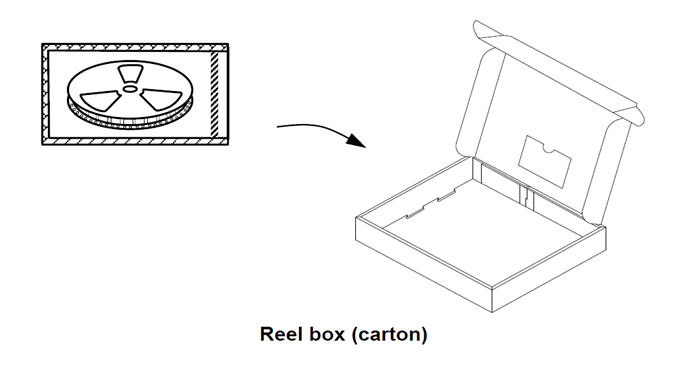
Reel Box
Each Moisture Barrier bag is packed into reel box.
-
Tape Structure
The carrier tape is made of plastic and the structure is shown in above schematic. The device is put on embossed area of carrier tape, and covered by cover tape made of plastic.

-
Reel Box Material
Corrugated Fiberboard