DLPS071A October   2015  – February 2023 DLPA3005

PRODUCTION DATA  

  1. Features
  2. Applications
  3. Description
  4. Revision History
  5. Pin Configuration and Functions
  6. Specifications
    1. 6.1 Absolute Maximum Ratings
    2. 6.2 ESD Ratings
    3. 6.3 Recommended Operating Conditions
    4. 6.4 Thermal Information
    5. 6.5 Electrical Characteristics
    6. 6.6 SPI Timing Parameters
  7. Detailed Description
    1. 7.1 Overview
    2. 7.2 Functional Block Description
    3. 7.3 Feature Description
      1. 7.3.1 Supply and Monitoring
        1. 7.3.1.1 Supply
        2. 7.3.1.2 Monitoring
          1. 7.3.1.2.1 Block Faults
          2. 7.3.1.2.2 Auto LED Turn Off Functionality
          3. 7.3.1.2.3 Thermal Protection
      2. 7.3.2 Illumination
        1. 7.3.2.1 Programmable Gain Block
        2. 7.3.2.2 LDO Illumination
        3. 7.3.2.3 Illumination Driver A
        4. 7.3.2.4 RGB Strobe Decoder
          1. 7.3.2.4.1 Break Before Make (BBM)
          2. 7.3.2.4.2 Openloop Voltage
          3. 7.3.2.4.3 Transient Current Limit
        5. 7.3.2.5 Illumination Monitoring
          1. 7.3.2.5.1 Power Good
          2. 7.3.2.5.2 Ratio Metric Overvoltage Protection
        6. 7.3.2.6 Illumination Driver plus Power FETs Efficiency
      3. 7.3.3 External Power FET Selection
        1. 7.3.3.1 Threshold Voltage
        2. 7.3.3.2 Gate Charge and Gate Timing
        3. 7.3.3.3 RDS(ON)
      4. 7.3.4 DMD Supplies
        1. 7.3.4.1 LDO DMD
        2. 7.3.4.2 DMD HV Regulator
        3. 7.3.4.3 DMD/DLPC Buck Converters
        4. 7.3.4.4 DMD Monitoring
          1. 7.3.4.4.1 Power Good
          2. 7.3.4.4.2 Overvoltage Fault
      5. 7.3.5 Buck Converters
        1. 7.3.5.1 LDO Bucks
        2. 7.3.5.2 General Purpose Buck Converter
        3. 7.3.5.3 Buck Converter Monitoring
          1. 7.3.5.3.1 Power Good
          2. 7.3.5.3.2 Overvoltage Fault
        4. 7.3.5.4 Buck Converter Efficiency
      6. 7.3.6 Auxiliary LDOs
      7. 7.3.7 Measurement System
    4. 7.4 Device Functional Modes
    5. 7.5 Programming
      1. 7.5.1 SPI
      2. 7.5.2 Interrupt
      3. 7.5.3 Fast-Shutdown in Case of Fault
      4. 7.5.4 Protected Registers
    6. 7.6 Register Maps
  8. Application and Implementation
    1. 8.1 Application Information
    2. 8.2 Typical Application
      1. 8.2.1 Design Requirements
      2. 8.2.2 Detailed Design Procedure
        1. 8.2.2.1 Component Selection for General-Purpose Buck Converters
      3. 8.2.3 Application Curve
    3. 8.3 System Example With DLPA3005 Internal Block Diagram
  9. Power Supply Recommendations
    1. 9.1 Power-Up and Power-Down Timing
  10. 10Layout
    1. 10.1 Layout Guidelines
      1. 10.1.1 SPI Connections
      2. 10.1.2 RLIM Routing
      3. 10.1.3 LED Connection
    2. 10.2 Layout Example
    3. 10.3 Thermal Considerations
  11. 11Device and Documentation Support
    1. 11.1 Device Support
      1. 11.1.1 Device Nomenclature
    2. 11.2 Third-Party Products Disclaimer
    3. 11.3 Related Links
    4. 11.4 Receiving Notification of Documentation Updates
    5. 11.5 Support Resources
    6. 11.6 Trademarks
    7. 11.7 Electrostatic Discharge Caution
    8. 11.8 Glossary
  12. 12Mechanical, Packaging, and Orderable Information
    1. 12.1 Package Option Addendum

Package Options

Mechanical Data (Package|Pins)
Thermal pad, mechanical data (Package|Pins)
Orderable Information

DMD Supplies

This block contains all the supplies needed for the DMD and DLPC (Figure 7-12). The block comprises:

  • LDO_DMD: for internal supply
  • DMD_HV: regulator generates high voltage supplies
  • Two buck converters: for DLPC/DMD voltages
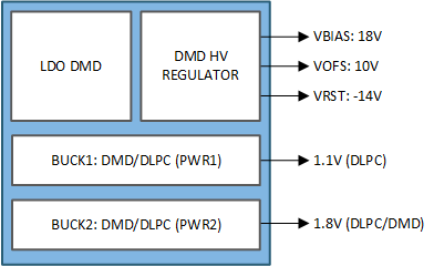
GUID-20221011-SS0I-HN2T-M9VN-R4JZDJMK9PQ6-low.gif Figure 7-12 DMD Supplies Blocks

The DMD supplies block is designed to work with the DMD and the related DLPC. The DMD has its own set of supply voltage requirements. Besides the three high voltages, two supplies are needed for the DMD and the related DLPC (DLPC343x-family for instance). These supplies are made by two buck converters.

The EEPROM of the DLPA3005 is factory programmed for a certain configuration, such as which buck converters are used. Which configuration is programmed in EEPROM can be read in the capability register. It concerns the following bits:

  • DMD_BUCK1_USE
  • DMD_BUCK2_USE