DLPS048C March 2015 – June 2019 DLPC150
PRODUCTION DATA.
- 1 Features
- 2 Applications
- 3 Description
- 4 Revision History
- 5 Pin Configuration and Functions
-
6 Specifications
- 6.1 Absolute Maximum Ratings
- 6.2 ESD Ratings
- 6.3 Recommended Operating Conditions
- 6.4 Thermal Information
- 6.5 Electrical Characteristics Over Recommended Operating Conditions
- 6.6 Electrical Characteristics
- 6.7 High-Speed Sub-LVDS Electrical Characteristics
- 6.8 Low-Speed SDR Electrical Characteristics
- 6.9 System Oscillators Timing Requirements
- 6.10 Power-Up and Reset Timing Requirements
- 6.11 Parallel Interface Frame Timing Requirements
- 6.12 Parallel Interface General Timing Requirements
- 6.13 Flash Interface Timing Requirements
- 7 Parameter Measurement Information
- 8 Detailed Description
- 9 Application and Implementation
- 10Power Supply Recommendations
-
11Layout
- 11.1
Layout Guidelines
- 11.1.1 PCB Layout Guidelines For Internal Controller PLL Power
- 11.1.2 DLPC150 Reference Clock
- 11.1.3 General PCB Recommendations
- 11.1.4 General Handling Guidelines for Unused CMOS-Type Pins
- 11.1.5 Maximum Pin-to-Pin, PCB Interconnects Etch Lengths
- 11.1.6 Number of Layer Changes
- 11.1.7 Stubs
- 11.1.8 Terminations
- 11.1.9 Routing Vias
- 11.2 Layout Example
- 11.3 Thermal Considerations
- 11.1
Layout Guidelines
- 12Device and Documentation Support
- 13Mechanical, Packaging, and Orderable Information
Package Options
Mechanical Data (Package|Pins)
- ZEZ|201
Thermal pad, mechanical data (Package|Pins)
8.3.5 DMD (Sub-LVDS) Interface
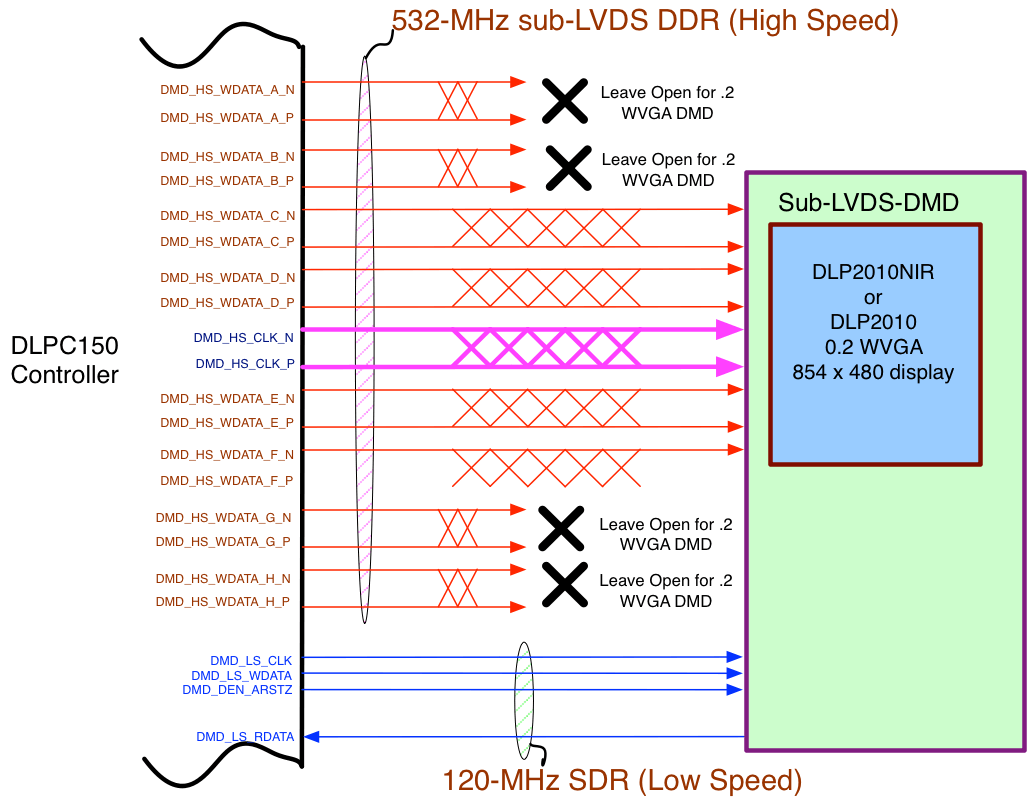
The DLPC150 controller DMD interface consists of a high speed 1.8-V sub-LVDS output only interface with a maximum clock speed of 532-MHz DDR and a low speed SDR (1.8-V LVCMOS) interface with a fixed clock speed of 120 MHz. The DLPC150 sub-LVDS interface supports a number of DMD display sizes, and as a function of resolution, not all output data lanes are needed as DMD display resolutions decrease in size. With internal software selection, the DLPC150 also supports a limited number of DMD interface swap configurations that can help board layout by remapping specific combinations of DMD interface lines to other DMD interface lines as needed. Table 9 shows the four options available for the DLP2010 or DLP2010NIR (0.2-inch WVGA) DMD. Any unused DMD signal pairs should be left unconnected on the final board design.
Table 9. DLP2010 or DLP2010NIR (0.2-Inch WVGA) DMD – Controller to 4-Lane DMD Pin Mapping Options
| DLPC150 CONTROLLER 4 LANE DMD ROUTING OPTIONS | DMD PINS | |||
|---|---|---|---|---|
| OPTION 1
SWAP CONTROL = x0 |
OPTION 2
SWAP CONTROl = x2 |
OPTION 3
SWAP CONTROL = x1 |
OPTION 4
SWAP CONTROL = x3 |
|
| HS_WDATA_D_P
HS_WDATA_D_N |
HS_WDATA_E_P
HS_WDATA_E_N |
HS_WDATA_H_P
HS_WDATA_H_N |
HS_WDATA_A_P
HS_WDATA_A_N |
Input DATA_p_0
Input DATA_n_0 |
| HS_WDATA_C_P
HS_WDATA_C_N |
HS_WDATA_F_P
HS_WDATA_F_N |
HS_WDATA_G_P
HS_WDATA_G_N |
HS_WDATA_B_P
HS_WDATA_B_N |
Input DATA_p_1
Input DATA_n_1 |
| HS_WDATA_F_P
HS_WDATA_F_N |
HS_WDATA_C_P
HS_WDATA_C_N |
HS_WDATA_B_P
HS_WDATA_B_N |
HS_WDATA_G_P
HS_WDATA_G_N |
Input DATA_p_2
Input DATA_n_2 |
| HS_WDATA_E_P
HS_WDATA_E_N |
HS_WDATA_D_P
HS_WDATA_D_N |
HS_WDATA_A_P
HS_WDATA_A_N |
HS_WDATA_H_P
HS_WDATA_H_N |
Input DATA_p_3
Input DATA_n_3 |
 Figure 11. DLP2010 Or DLP2010NIR (0.2-Inch WVGA) DMD Interface Example (Mapping Option 1 Shown)