SLDS227 March 2016 DRV10964
PRODUCTION DATA.
- 1 Features
- 2 Applications
- 3 Description
- 4 Revision History
- 5 Pin Configuration and Functions
- 6 Specifications
-
7 Detailed Description
- 7.1 Overview
- 7.2 Functional Block Diagram
- 7.3 Feature Description
- 7.4 Device Functional Modes
- 8 Application and Implementation
- 9 Power Supply Recommendations
- 10Layout
- 11Device and Documentation Support
- 12Mechanical, Packaging, and Orderable Information
Package Options
Mechanical Data (Package|Pins)
- DSN|10
Thermal pad, mechanical data (Package|Pins)
- DSN|10
Orderable Information
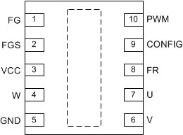
5 Pin Configuration and Functions
DSN Package
10-Pin USON
Top View

Pin Functions
| PIN | I/O | DESCRIPTION | |
|---|---|---|---|
| NO. | NAME | ||
| 1 | FG | Output | Motor speed indicator output (open drain). |
| 2 | FGS | Input | Motor speed indicator selector. The state of this pin is latched on power up and can not be changed dynamically. |
| 3 | VCC | Power | Input voltage for motor and chip supply. |
| 4 | W | IO | Motor Phase W |
| 5 | GND | Ground | Ground |
| 6 | V | IO | Motor Phase V |
| 7 | U | IO | Motor Phase U |
| 8 | FR | Input | Motor direction selector. This pin can be dynamically changed after power up. |
| 9 | CONFIG | Input | Resistor setting for configuring the handoff threshold. The state of this pin is latched on power up and can not be changed dynamically. |
| 10 | PWM | Input | Motor speed control input. |
| — | Thermal Pad | — | Connect to Ground for maximum thermal efficiency. Thermal pad is on the bottom of the package. |