SLOS879B April 2014 – September 2016 DRV2625
PRODUCTION DATA.
- 1 Features
- 2 Applications
- 3 Description
- 4 Revision History
- 5 Pin Configuration and Functions
- 6 Specifications
- 7 Parameter Measurement Information
-
8 Detailed Description
- 8.1 Overview
- 8.2 Functional Block Diagram
- 8.3
Feature Description
- 8.3.1 Support for ERM and LRA Actuators
- 8.3.2 Smart-Loop Architecture
- 8.3.3 Open-Loop Operation
- 8.3.4 Flexible Front-End Interface
- 8.3.5 Noise Gate Control
- 8.3.6 Edge Rate Control
- 8.3.7 Constant Vibration Strength
- 8.3.8 Battery Voltage Reporting
- 8.3.9 Ultra Low-Power Shutdown
- 8.3.10 Automatic Go-To-Stand-by (Low Power)
- 8.3.11 I2C Watchdog Timer
- 8.3.12 Device Protection
- 8.3.13 POR
- 8.3.14 Silicon Revision Control
- 8.3.15 Support for LRA and ERM Actuators
- 8.3.16 Multi-Purpose Pin Functionality
- 8.3.17 Automatic Transition to Standby State
- 8.3.18 Automatic Brake into Standby
- 8.3.19 Battery Monitoring and Power Preservation
- 8.4 Device Functional Modes
- 8.5 Operation During Exceptional Conditions
- 8.6
Programming
- 8.6.1 Auto-Resonance Engine Programming for the LRA
- 8.6.2 Automatic-Level Calibration Programming
- 8.6.3 I2C Interface
- 8.6.4 Programming for Open-Loop Operation
- 8.6.5 Programming for Closed-Loop Operation
- 8.6.6 Diagnostics Routine
- 8.6.7 Calibration Routine
- 8.6.8 Waveform Playback Programming
- 8.6.9 Waveform Setup and Playback
- 8.7
Register Map
- 8.7.1 Address: 0x00
- 8.7.2 Address: 0x01
- 8.7.3 Address: 0x02
- 8.7.4 Address: 0x03
- 8.7.5 Address: 0x04
- 8.7.6 Address: 0x05
- 8.7.7 Address: 0x06
- 8.7.8 Address: 0x07
- 8.7.9 Address: 0x08
- 8.7.10 Address: 0x09
- 8.7.11 Address: 0x0A
- 8.7.12 Address: 0x0B
- 8.7.13 Address: 0x0C
- 8.7.14 Address: 0x0D
- 8.7.15 Address: 0x0E
- 8.7.16 Address: 0x0F
- 8.7.17 Address: 0x10
- 8.7.18 Address: 0x11
- 8.7.19 Address: 0x12
- 8.7.20 Address: 0x13
- 8.7.21 Address: 0x14
- 8.7.22 Address: 0x15
- 8.7.23 Address: 0x16
- 8.7.24 Address: 0x17
- 8.7.25 Address: 0x18
- 8.7.26 Address: 0x19
- 8.7.27 Address: 0x1A
- 8.7.28 Address: 0x1B
- 8.7.29 Address: 0x1C
- 8.7.30 Address: 0x1D
- 8.7.31 Address: 0x1F
- 8.7.32 Address: 0x20
- 8.7.33 Address: 0x21
- 8.7.34 Address: 0x22
- 8.7.35 Address: 0x23
- 8.7.36 Address: 0x24
- 8.7.37 Address: 0x25
- 8.7.38 Address: 0x26
- 8.7.39 Address: 0x27
- 8.7.40 Address: 0x28
- 8.7.41 Address: 0x29
- 8.7.42 Address: 0x2A
- 8.7.43 Address: 0x2C
- 8.7.44 Address: 0x2E
- 8.7.45 Address: 0x2F
- 8.7.46 Address: 0x30
- 9 Application and Implementation
- 10Power Supply Recommendations
- 11Layout
- 12Device and Documentation Support
- 13Mechanical, Packaging, and Orderable Information
Package Options
Refer to the PDF data sheet for device specific package drawings
Mechanical Data (Package|Pins)
- YFF|9
Thermal pad, mechanical data (Package|Pins)
Orderable Information
6 Specifications
6.1 Absolute Maximum Ratings
over operating free-air temperature range (unless otherwise noted) (1)| MIN | MAX | UNIT | ||
|---|---|---|---|---|
| Supply Voltage | VDD | –0.3 | 6 | V |
| Input voltage | NRST | –0.3 | 6 | V |
| SDA | –0.3 | 6 | V | |
| SCL | –0.3 | 6 | V | |
| TRIG/INTZ | –0.3 | 6 | V | |
| Operating free-air temperature range, TA | –40 | 85 | °C | |
| Operating junction temperature range, TJ | –40 | 150 | °C | |
| Storage temperature, Tstg | –65 | 150 | °C | |
(1) Stresses beyond those listed under Absolute Maximum Ratings may cause permanent damage to the device. These are stress ratings only, which do not imply functional operation of the device at these or any other conditions beyond those indicated under Recommended Operating Conditions. Exposure to absolute-maximum-rated conditions for extended periods may affect device reliability.
6.2 ESD Ratings
| MIN | MAX | UNIT | |||
|---|---|---|---|---|---|
| V(ESD) | Electrostatic discharge | Human body model (HBM), per ANSI/ESDA/JEDEC JS-001, all pins(1) | –1500 | 1500 | V |
| Charged device model (CDM), per JEDEC specification JESD22-C101, all pins(2) | –500 | 500 | |||
(1) JEDEC document JEP155 states that 500-V HBM allows safe manufacturing with a standard ESD control process.
(2) JEDEC document JEP157 states that 250-V CDM allows safe manufacturing with a standard ESD control process.
6.3 Recommended Operating Conditions
over operating free-air temperature range (unless otherwise noted)| MIN | NOM | MAX | UNIT | ||
|---|---|---|---|---|---|
| VDD | Supply voltage | 2.7 | 5.5 | V | |
| RL | Load impedance | 8 | Ω | ||
| CL | Load capacitance | 100 | pF | ||
| ƒ(LRA) | LRA frequency | 45 | 300 | Hz | |
6.4 Thermal Information
| THERMAL METRIC(1) | DRV2625 | UNIT | |
|---|---|---|---|
| DSBGA | |||
| 9 PINS | |||
| RθJA | Junction-to-ambient thermal resistance | 107 | °C/W |
| RθJC(top) | Junction-to-case (top) thermal resistance | 0.9 | °C/W |
| RθJB | Junction-to-board thermal resistance | 18.1 | °C/W |
| ψJT | Junction-to-top characterization parameter | 3.8 | °C/W |
| ψJB | Junction-to-board characterization parameter | 18.1 | °C/W |
| RθJC(bot) | Junction-to-case (bottom) thermal resistance | — | °C/W |
(1) For more information about traditional and new thermal metrics, see the Semiconductor and IC Package Thermal Metrics application report, SPRA953.
6.5 Electrical Characteristics
TA = 25 °C, VDD = 3.6 V (unless otherwise noted)| PARAMETER | TEST CONDITIONS | MIN | TYP | MAX | UNIT | |
|---|---|---|---|---|---|---|
| V(REG) | Voltage at the REG pin | 1.84 | V | |||
| IIL | Digital low-level input current | NRST, TRIG/INTZ, SDA, SCL VDD = 5.5 V, VI = 0 V |
100 | nA | ||
| IIH | Digital high-level input current | SDA, SCL VDD = 5.5 V, VI = VDD |
0.1 | µA | ||
| NRST VDD = 5.5 V, VI = VDD |
1 | |||||
| TRIG/INTZ VDD = 5.5 V, VI = VDD |
2.7 | 3.5 | ||||
| VIL | Digital low-level input voltage | NRST, TRIG/INTZ, SDA, SCL | 0.4 | V | ||
| VIH | Digital high-level input voltage | NRST, TRIG/INTZ, SDA, SCL | 1.41 | V | ||
| VOL | Digital low-level output voltage | TRIG/INTZ, SDA 3-mA sink current |
0.4 | V | ||
| RDS(on) | Drain-source on-state resistance (LS + HS) | 0.75 | Ω | |||
| I(SD) | Shutdown current | V(NRST) = 0 V | 105 | 180 | nA | |
| I(STBY) | Standby current | V(NRST) = VDD
In stand-by mode |
1.55 | 2 | µA | |
| I(Q) | Quiescent current | V(NRST) = VDD
In idle mode - no signal |
2.5 | mA | ||
| ZO(SD) | Output impedance in shutdown | OUT+ to GND, OUT– to GND | 15 | kΩ | ||
| ZO(STBY) | Output impedance in standby | OUT+ to GND, OUT– to GND | 15 | kΩ | ||
| ZLOAD(th) | Load impedance threshold for over-current detection | OUT+ to GND, OUT– to GND | 4 | Ω | ||
6.6 Timing Requirements
TA = 25 °C, VDD = 3.6 V (unless otherwise noted)| MIN | NOM | MAX | UNIT | ||
|---|---|---|---|---|---|
| ƒ(SCL) | Frequency at the SCL pin with no wait states | 400 | kHz | ||
| tw(H) | Pulse duration, SCL high | 0.6 | µs | ||
| tw(L) | Pulse duration, SCL low | 1.3 | µs | ||
| tsu(1) | Setup time, SDA to SCL | 100 | ns | ||
| th(1) | Hold time, SCL to SDA | 10 | ns | ||
| t(BUF) | Bus free time between stop and start condition | 1.3 | µs | ||
| tsu(2) | Setup time, SCL to start condition | 0.6 | µs | ||
| th(2) | Hold time, start condition to SCL | 0.6 | µs | ||
| tsu(3) | Setup time, SCL to stop condition | 0.6 | µs | ||
6.7 Switching Characteristics
TA = 25 °C, VDD = 3.6 V (unless otherwise noted)| PARAMETER | TEST CONDITIONS | MIN | TYP | MAX | UNIT | |
|---|---|---|---|---|---|---|
| t(on) | Device startup time | from shutdown standby | 1 | ms | ||
| t(start) | Waveform startup time | from trigger to output signal | 1 | ms | ||
| fO(PWM) | PWM output frequency (in OUT+ and OUT-) | 20.5 | kHz | |||
 Figure 1. SCL and SDA Timing
 Figure 2. Timing for Start and Stop Conditions
6.8 Typical Characteristics
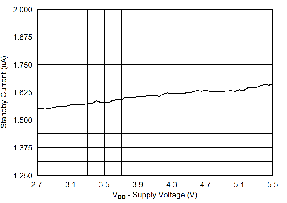
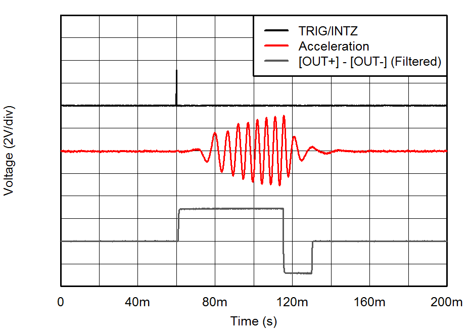
| VDD = 3.6 V | |
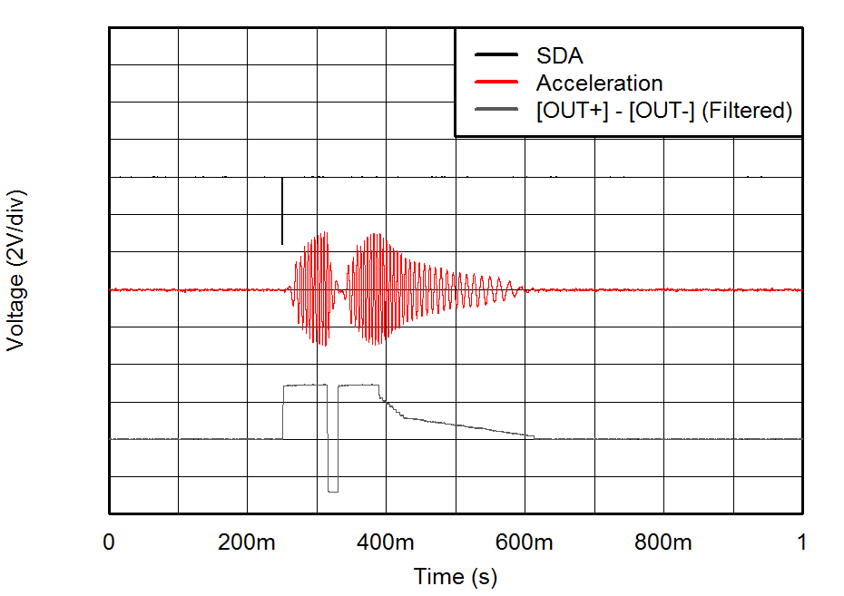
| VDD = 3.6 V | |
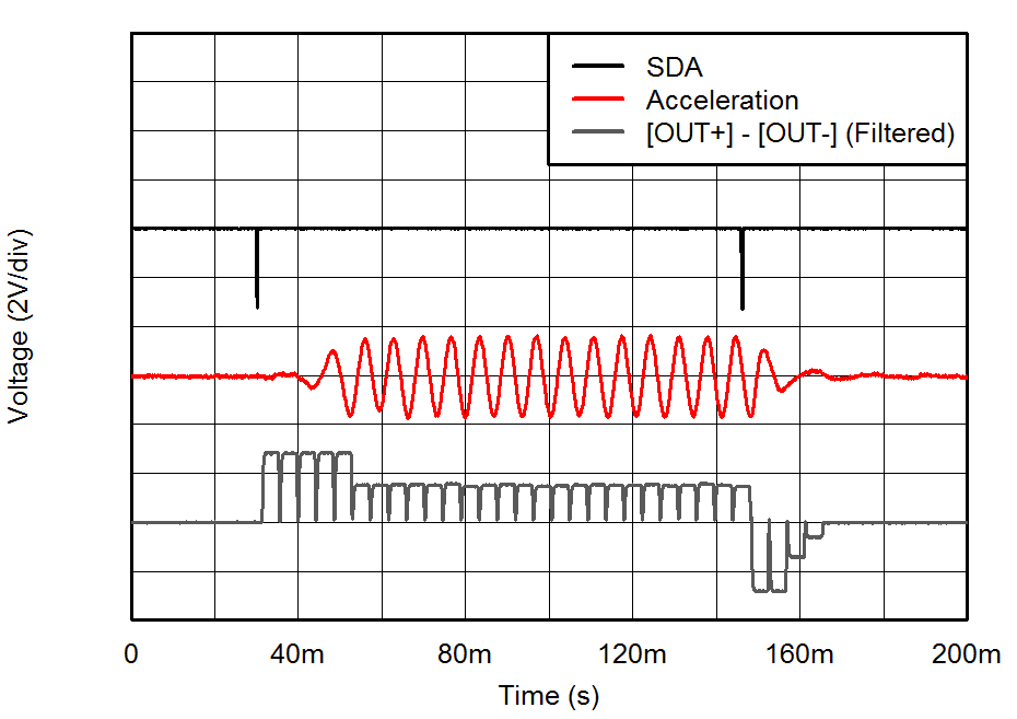
| VDD = 3.6 V | |

| VDD = 3.6 V | |
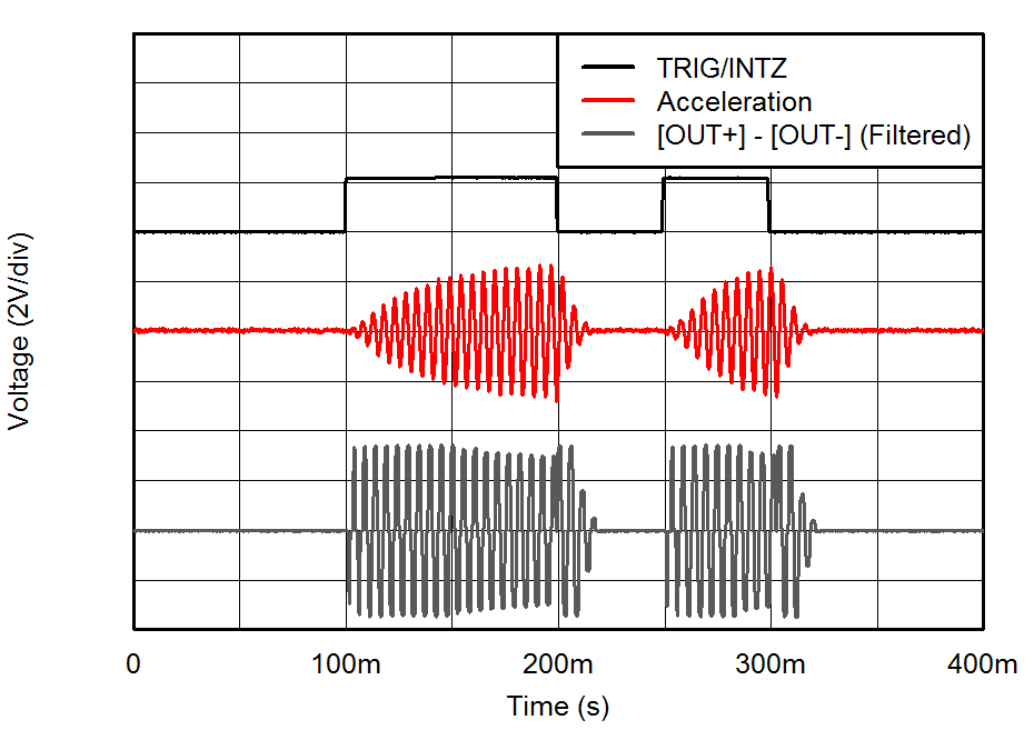
| VDD = 3.6 V | |
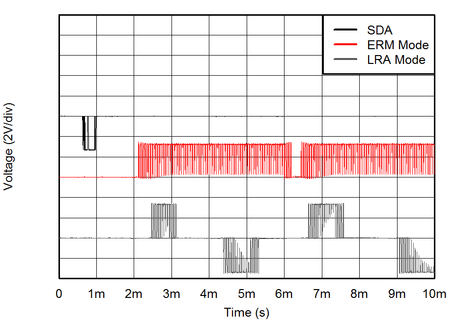
| VDD = 3.6 V | |
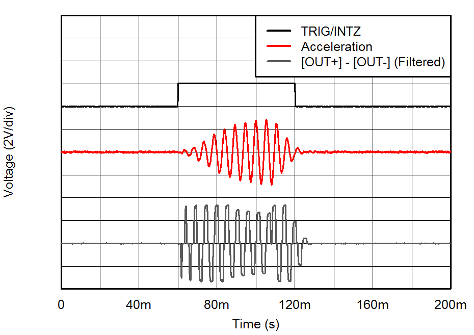
| VDD = 3.6 V | |
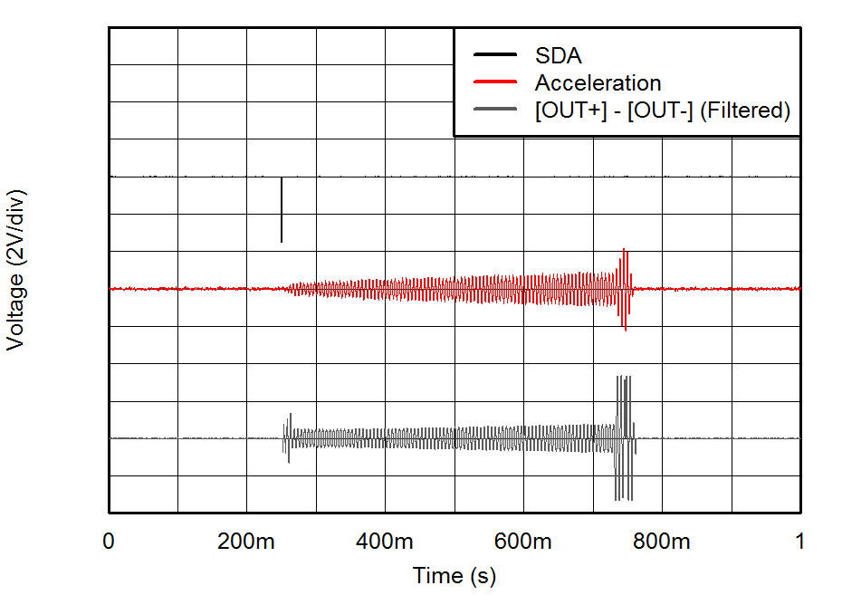
| VDD = 3.6 V | |
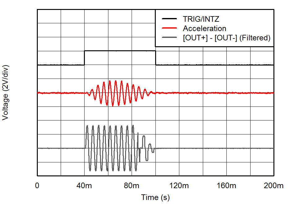
| VDD = 3.6 V | |
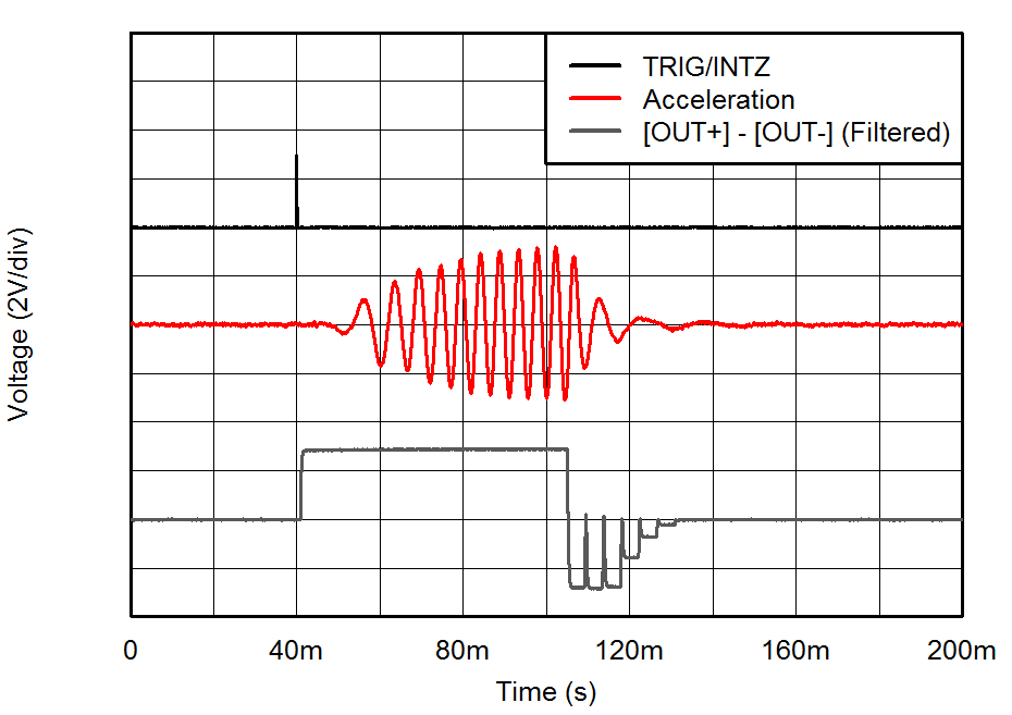
| VDD = 3.6 V | |
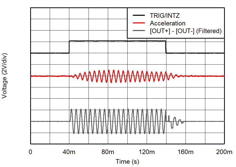
| VDD = 3.6 V | |