SLIS154A December 2014 – December 2015 DRV5053-Q1
PRODUCTION DATA.
- 1 Features
- 2 Applications
- 3 Description
- 4 Revision History
- 5 Pin Configuration and Functions
- 6 Specifications
- 7 Detailed Description
- 8 Application and Implementation
- 9 Power Supply Recommendations
- 10Device and Documentation Support
- 11Mechanical, Packaging, and Orderable Information
Package Options
Mechanical Data (Package|Pins)
Thermal pad, mechanical data (Package|Pins)
Orderable Information
10 Device and Documentation Support
10.1 Device Support
10.1.1 Device Nomenclature
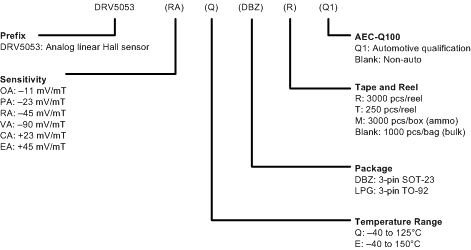
Figure 17 shows a legend for reading the complete device name for the DRV5053-Q1 device.
10.1.2 Device Markings
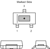
 Figure 18. SOT-23 (DBZ) Package
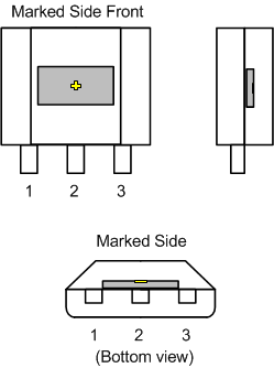
 Figure 19. TO-92 (LPG) Package
 indicates the Hall effect sensor (not to scale). The Hall element is located in the center of the package with a tolerance of ±100 µm. The height of the Hall element from the bottom of the package is 0.7 mm ±50 µm in the DBZ package and 0.987 mm ±50 µm in the LPG package.
10.2 Community Resources
The following links connect to TI community resources. Linked contents are provided "AS IS" by the respective contributors. They do not constitute TI specifications and do not necessarily reflect TI's views; see TI's Terms of Use.
-
TI E2E™ Online Community TI's Engineer-to-Engineer (E2E) Community. Created to foster collaboration among engineers. At e2e.ti.com, you can ask questions, share knowledge, explore ideas and help solve problems with fellow engineers.
-
Design Support TI's Design Support Quickly find helpful E2E forums along with design support tools and contact information for technical support.
10.3 Trademarks
E2E is a trademark of Texas Instruments.
All other trademarks are the property of their respective owners.
10.4 Electrostatic Discharge Caution

These devices have limited built-in ESD protection. The leads should be shorted together or the device placed in conductive foam during storage or handling to prevent electrostatic damage to the MOS gates.
10.5 Glossary
SLYZ022 — TI Glossary.
This glossary lists and explains terms, acronyms, and definitions.
