SLVSD12D May 2015 – July 2019 DRV8305-Q1
PRODUCTION DATA.
- 1 Features
- 2 Applications
- 3 Description
- 4 Revision History
- 5 Pin Configuration and Functions
- 6 Specifications
-
7 Detailed Description
- 7.1 Overview
- 7.2 Functional Block Diagram
- 7.3
Feature Description
- 7.3.1 Integrated Three-Phase Gate Driver
- 7.3.2 INHx/INLx: Gate Driver Input Modes
- 7.3.3 VCPH Charge Pump: High-Side Gate Supply
- 7.3.4 VCP_LSD LDO: Low-Side Gate Supply
- 7.3.5 GHx/GLx: Half-Bridge Gate Drivers
- 7.3.6 DVDD and AVDD: Internal Voltage Regulators
- 7.3.7 VREG: Voltage Regulator Output
- 7.3.8 Protection Features
- 7.3.9 Undervoltage Warning (UVFL), Undervoltage Lockout (UVLO), and Overvoltage (OV) Protection
- 7.4 Device Functional Modes
- 7.5 Programming
- 7.6
Register Maps
- 7.6.1 Status Registers
- 7.6.2
Control Registers
- 7.6.2.1 HS Gate Drive Control (Address = 0x5)
- 7.6.2.2 LS Gate Drive Control (Address = 0x6)
- 7.6.2.3 Gate Drive Control (Address = 0x7)
- 7.6.2.4 IC Operation (Address = 0x9)
- 7.6.2.5 Shunt Amplifier Control (Address = 0xA)
- 7.6.2.6 Voltage Regulator Control (Address = 0xB)
- 7.6.2.7 VDS Sense Control (Address = 0xC)
- 8 Application and Implementation
- 9 Power Supply Recommendations
- 10Layout
- 11Device and Documentation Support
- 12Mechanical, Packaging, and Orderable Information
Package Options
Mechanical Data (Package|Pins)
- PHP|48
Thermal pad, mechanical data (Package|Pins)
- PHP|48
Orderable Information
7.3.5.3 CSAs: Current Shunt Amplifiers
The DRV8305-Q1 includes three high performance low-side current shunt amplifiers for accurate current measurement utilizing low-side shunt resistors in the external half-bridges. They are commonly used to measure the motor phase current to implement overcurrent protection, external torque control, or external commutation control through the application MCU.
The current shunt amplifiers have the following features:
- Each of the three current sense amplifiers can be programmed and calibrated independently.
- Can provide output bias up to 2.5 V to support bidirectional current sensing.
- May be used for either individual or total current shunt sensing.
- Four programmable gain settings through SPI registers (10, 20, 40 and 80 V/V).
- Reference voltage for output bias provided from voltage regulator VREG for DRV83053Q and DRV83055Q.
- Reference voltage for output bias provided from externally applied voltage on VREG pin for DRV8305NQ and DRV8305NE.
- Programmable output bias scaling. The scaling factor k can be programmed through SPI registers (1/2 or 1/4).
- Programmable blanking time (delay) of the amplifier outputs. The blanking time is implemented from any rising or falling edge of gate drive outputs. The blanking time is applied to all three current sense amplifiers equally. In case the current sense amplifiers are already being blanked when another gate driver rising or falling edge is seen, the blanking interval will be restarted at the edge. Note that the blanking time options do not include delay from internal amplifier loading or delays from the trace or component loads on the amplifier output. The programmable blanking time may be overridden to have no delay (default value).
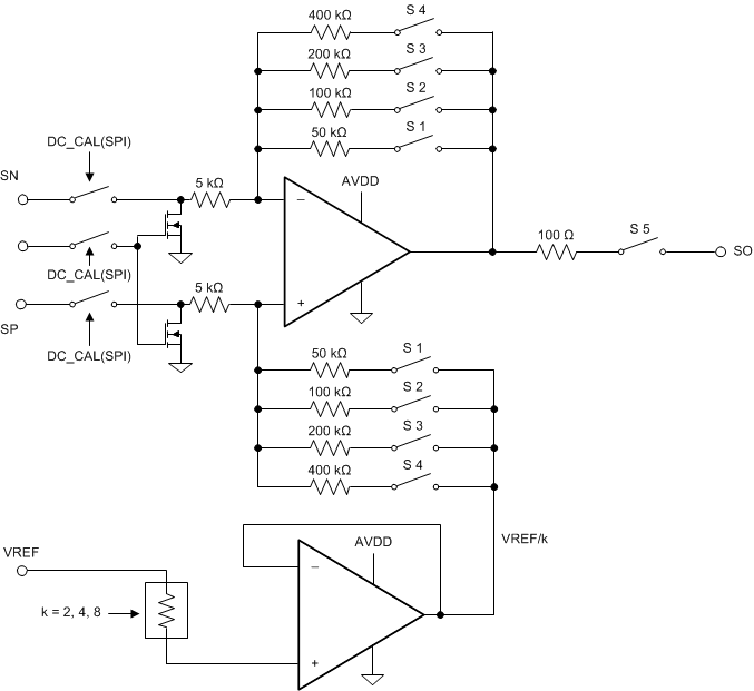
- Minimize DC offset and drift through temperature with DC calibrating through SPI register. When DC calibration is enabled, device will short input of current shunt amplifier and disconnect the load. DC calibrating can be done at anytime, even when the MOSFET is switching because the load is disconnected. For best result, perform the DC calibrating during switching off period when no load is present to reduce the potential noise impact to the amplifier.
The output of current shunt amplifier can be calculated as:
Equation 1. 

where
- VREF is the reference voltage from the VREG pin.
- G is the gain setting of the amplifier.
- k = 2, 4, or 8
- SNx and SPx are the inputs of channel x.
- SPx should connect to the low-side (ground) of the sense resistor for the best common mode rejection.
- SNx should connect to the high-side (LS MOSFET source) of the sense resistor.
Figure 12 shows current amplifier simplified block diagram.
 Figure 12. Current Shunt Amplifier Simplified Block Diagram